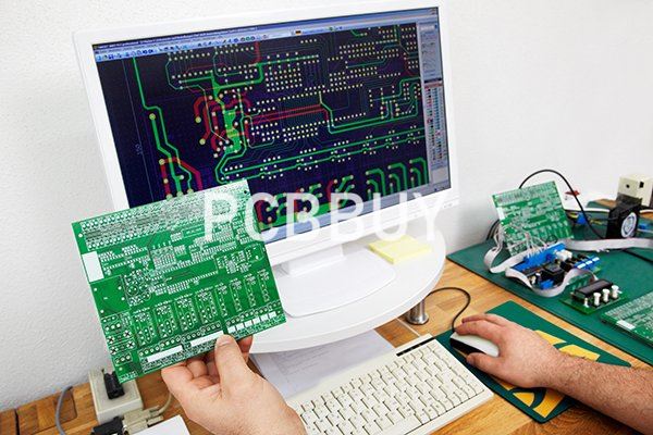
How to Make Custom PCB Board with 5 Effective Tips?
By:PCBBUY 10/18/2021 10:19

Printed circuit boards (PCBs) solve all those shortcomings. But most people don’t even consider translating a one-off project into a PCB design. For one thing, PCB fabrication has traditionally been expensive, viable only in commercial quantities. Also, there are technical constraints involved with PCB designs that are daunting to the casual hobbyist.
Want to know what are the tips of custom PCB? In this passage, we are going to provide you everything about how to custom PCB. If you are interested in this topic, please check and read this passage for more information.
1. How to prepare PCB design before custom PCB?
Identify what each part of your circuit does, and divide the circuit into sections according to function. For example, my LM386 audio amplifier circuit has four main sections: a power supply, an audio input, the LM386, and an audio output. It might help to draw some diagrams at this point to help you visualize the design before you start laying it out.
Keep the components in each section grouped together in the same area of the PCB to keep the conductive traces short. Long traces can pick up electromagnetic radiation from other sources, which can cause interference and noise.
2. How to create Gerber files for custom PCB?
The first step in getting the Maker Pro robot PCB manufactured is creating Gerber format design files from Eagle. There are, of course, many different options for PCB design software available to makers and engineers. Each has its own internal PCB format; in the case of Autodesk Eagle, we use .SCH files for schematics and .BRD files for boards.
The Gerber format, on the other hand, is a standardized, open format that can be exported from any PCB design software. Gerbers are the standard file format used in the PCB manufacturing industry.

3. How to determine the price for custom PCB?
One of the first major steps on the road to bringing a new product to market is the creation of a prototype. Learn just how much the prototyping process is going to cost you. The cost of a prototype can be broken into two major parts: the engineering cost to design it, and the actual cost to produce it.
The total cost of the prototype (assuming an electronic product) usually includes the cost to manufacture the custom Printed Circuit Board (PCB), plus the cost of components, assembly, and the enclosure. For most products the engineering costs will dominate. They also can vary greatly depending on several variables but especially on the product complexity.
Engineering fees may be only a few thousand dollars for a simple product up to hundreds of thousands of dollars for a really complex product.
Ultimately, the best way to reduce your prototyping cost (in fact, all of your costs) is to simplify your product as much as possible as early as possible. Many times a seemingly “simple” feature can dramatically increase the development complexity and cost.
4. How to choose a PCB manufacturer?
This is by no means an attempt to provide a comprehensive list of fab houses that you might want to use for a low-quantity order; that information is readily available via Google. Instead, I want to offer some suggestions based on my knowledge and experience. I’m not going to comment on the quality of the boards produced by a given manufacturer because I’ve never in my life received a PCB that I would describe as poorly manufactured (I don’t know if this is because I’m lucky or because I have a knack for identifying fab houses that are serious about quality). I think it’s safe to assume that all of the following fab houses will deliver a fully functional PCB.
5. How to determine a professional PCBA?
The primary obstacle here is cost. Automated assembly technology is mature and highly reliable, but the process is not economically adapted to low-quantity orders. It also requires additional manufacturing data:

· BOM information: The assembly house needs information that enables them to either order the parts or organize the parts that you provide.
· Solder mask: You need to submit Gerber files that identify the areas of the board (e.g., pads for IC pins) that must receive solder during the process of solder-paste deposition. (Solder paste is the type of solder used in reflow assembly.) This can be a bit complicated because in some cases you need to create solder-mask divisions that divide one large pad into multiple smaller rectangles of solder paste (see this article for more information).
· Placement data: This includes spatial coordinates and rotation for every part on the board. The machine cannot place components if it doesn’t know which ones go where and how they are oriented.
Industry Category


