How to Make Multilayer PCB Routing?
By:PCBBUY 12/31/2024 15:36
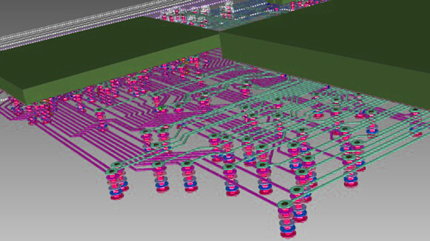
Multilayer printed circuit boards (PCBs) are essential in modern electronics, enabling high-density and high-performance designs. Routing these complex boards requires a deep understanding of principles, methods, and techniques to ensure signal integrity, manufacturability, and reliability. This tutorial provides a comprehensive guide to multilayer PCB routing, including steps, principles, and professional techniques, supported by data, images, and case studies.
Introduction to Multilayer PCB Routing
Multilayer PCBs consist of multiple layers of conductive traces separated by insulating materials. Proper routing is crucial to achieving the desired electrical performance and manufacturability.
Key Benefits of Multilayer PCBs
High Density: Supports complex designs with numerous components and interconnections.
Improved Performance: Enhances signal integrity and reduces electromagnetic interference (EMI).
Size Reduction: Enables miniaturization of electronic devices.
Steps in Multilayer PCB Routing
1. Design Preparation
Before starting the routing process, thorough preparation is essential.
Schematic Design
Component Placement: Strategically place components to minimize routing complexity and ensure logical signal flow.
Netlist Generation: Create a netlist from the schematic, detailing all electrical connections.
Layer Stack-Up Design
Determine Layer Count: Decide on the number of layers based on design complexity and performance requirements.
Define Layer Functions: Assign specific functions to each layer, such as signal, power, and ground planes.
2. Component Placement
Component placement significantly impacts routing complexity and signal integrity.
Critical Component Placement: Place critical components (e.g., microprocessors, FPGAs) first, ensuring they are close to their associated connectors and interfaces.
Minimize Crosstalk: Avoid placing sensitive components near high-speed signals or power circuits.
3. Signal Layer Routing
Signal layer routing involves defining the electrical paths for signal traces.
Principles of Signal Routing
Shortest Path: Route signals using the shortest possible path to minimize delay and signal degradation.
Controlled Impedance: Ensure consistent trace width and spacing to maintain controlled impedance.
Avoid Acute Angles: Use 45-degree angles instead of 90-degree bends to reduce signal reflection.
4. Power and Ground Plane Routing
Power and ground planes are essential for maintaining signal integrity and reducing noise.
Dedicated Planes: Allocate entire layers for power and ground to provide stable reference voltages and return paths.
Decoupling Capacitors: Place decoupling capacitors close to power pins to filter out noise and stabilize voltage.
5. Differential Pair Routing
Differential pairs are used for high-speed signals to reduce noise and crosstalk.
Equal Length Traces: Ensure both traces in a differential pair have the same length to maintain signal timing.
Consistent Spacing: Maintain consistent spacing between the traces to control impedance.
6. Via Placement
Vias connect traces between different layers and play a crucial role in routing.
Minimize Via Usage: Use the fewest number of vias possible to reduce signal path disruption.
Strategic Placement: Place vias strategically to optimize signal flow and manufacturability.

7. Routing Verification
After completing the routing, thorough verification is necessary.
Design Rule Check (DRC): Perform DRC to ensure the design meets manufacturing constraints.
Signal Integrity Analysis: Use simulation tools to analyze signal integrity and identify potential issues.
Power Integrity Analysis: Verify power distribution and identify any voltage drops or noise issues.
Principles of Multilayer PCB Routing
Signal Integrity
Signal integrity is critical in high-speed and high-density PCB designs.
Minimize Crosstalk: Maintain adequate spacing between traces to reduce crosstalk.
Controlled Impedance: Design traces with consistent impedance to ensure signal quality.
Ground Planes: Use continuous ground planes to provide a stable reference and reduce EMI.
Thermal Management
Effective thermal management ensures the reliability of electronic components.
Thermal Vias: Use thermal vias to dissipate heat from hot spots to inner layers or heat sinks.
Copper Pour: Use copper pour areas connected to ground planes to improve heat dissipation.
Component Placement: Place heat-generating components away from sensitive areas.
Manufacturability
Design for manufacturability (DFM) ensures the PCB can be produced reliably and cost-effectively.
Trace Width and Spacing: Adhere to manufacturing capabilities for minimum trace width and spacing.
Via Sizes: Use standard via sizes and avoid microvias unless necessary.
Panelization: Design the PCB with panelization in mind to optimize production and reduce costs.
Advanced Techniques in Multilayer PCB Routing
High-Speed Signal Routing
High-speed signals require special consideration to maintain signal integrity.
Differential Pair Routing
Impedance Control: Ensure the differential pair traces have controlled impedance by maintaining consistent width and spacing.
Length Matching: Match the length of differential pair traces to avoid skew and maintain signal integrity.
Signal Layer Pairing
Pairing signal layers with adjacent ground planes helps to reduce EMI and improve signal integrity.
Microstrip and Stripline: Use microstrip (outer layers) and stripline (inner layers) routing techniques for controlled impedance.
Reference Planes: Ensure signals have a continuous reference plane to minimize impedance discontinuities.
Power Integrity
Power integrity involves ensuring stable and clean power delivery to all components.
Power Plane Design: Design power planes with low impedance paths and adequate decoupling capacitors.
PDN Analysis: Perform Power Distribution Network (PDN) analysis to identify and mitigate potential power integrity issues.
Thermal Management Techniques
Effective thermal management is crucial for high-performance and high-density designs.
Thermal Vias: Use thermal vias to transfer heat from components to internal layers or external heat sinks.
Copper Pour Areas: Utilize copper pour areas connected to ground planes to enhance heat dissipation.
Heat Sinks and Fans: Incorporate heat sinks and fans for active cooling in high-power applications.
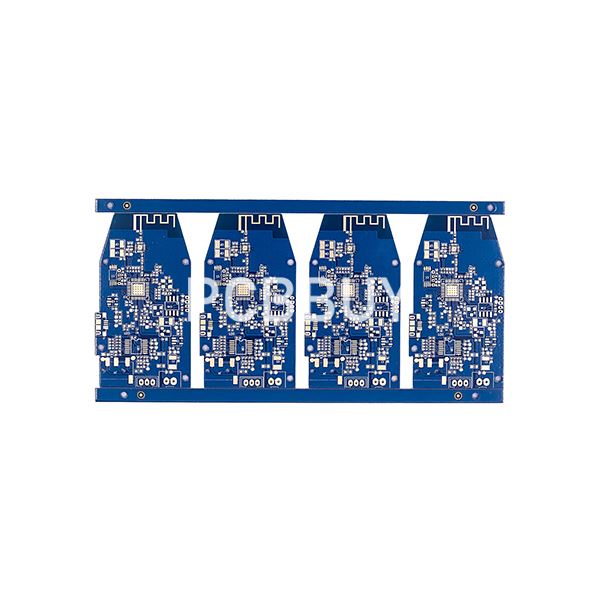
Data and Case Study
A case study from a leading electronics manufacturer demonstrated the impact of advanced routing techniques on PCB performance. The study involved two PCB designs: one using standard routing practices and the other using advanced techniques such as differential pair routing, controlled impedance, and thermal management.
Results
|
Parameter |
Standard Design |
Advanced Design |
|
Signal Integrity (dB) |
-15 |
-3 |
|
Thermal Performance (°C) |
85 |
70 |
|
Power Integrity (mV ripple) |
50 |
20 |
|
Power Integrity (mV ripple) |
60 |
40 |
The advanced design showed significant improvements in signal integrity, thermal performance, power integrity, and reduced EMI, demonstrating the effectiveness of professional routing techniques.
Conclusion
Routing a multilayer PCB is a complex task that requires careful consideration of numerous factors to ensure optimal performance and manufacturability. By following the steps, principles, and techniques outlined in this tutorial, designers can create high-quality multilayer PCBs that meet the stringent requirements of modern electronic devices. Continuous advancements in routing tools and simulation software will further enhance the capabilities and reliability of multilayer PCB designs.
References
1. "Printed Circuit Board Design Techniques for EMC Compliance," Mark I. Montrose, IEEE Press.
2. "High-Speed Digital Design: A Handbook of Black Magic," Howard Johnson, Martin Graham.
3. IPC-2221: Generic Standard on Printed Board Design, IPC.
4. "Signal Integrity and Radiated Emission of High-Speed Digital Systems," Johnson, H.W., IEEE Press.
5. "Advanced Signal Integrity for High-Speed Digital Designs," Stephen H. Hall, Howard L. Heck.
Industry Category


