How to Make Multilayer PCB with 9 Manufacturing Process Steps?
By:PCBBUY 09/28/2021 09:17

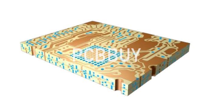
PCB is one of the most important parts of electronic circuits and contribute to their performance. Certainly, along with the operations of PCBs, it becomes important to understand their manufacturing process as well. Since 60% of PCBs used in the industrial electronic circuits are multilayered, the manufacturing process of multilayer PCB becomes a topic of interest. The demand for smaller, powerful, and faster devices has driven the demand for multilayer PCBs.
In this passage, we will tell you about all the details of multilayer PCB manufacturing process. And if you are interested in the manufacturing process of multilayer PCB, please check and read the content below for more professional knowledge.
What are the benefits of multilayer PCB?
· Higher assembly density
· Smaller size (considerable savings on space)
· Increased flexibility
· Easier incorporation controlled impedance features.
· EMI shielding through careful placement of power and ground layers.
· Reduces the need for interconnection wiring harnesses
How to make multilayer PCB with 9 steps?
The manufacturing steps for PCBAs are basically the same for all construction types with some important distinctions. Specific issues for board fabrication and PCB assembly that are common for multilayer designs are as follows:
1. What is Cut?
Cutting is the process of cutting the original copper-clad board into a board that can be made on the production line.
Generally, the purchased materials come in the following sizes: 36.5 INCH × 48.5 INCH, 40.5INCH X 48.5 INCH, 42.5 INCH X 48.5 INCH, etc. PCB design engineers and PCB production engineers always consider how to maximize the use of PCB raw materials throughout the process.
2. What is Inner dry film?
The inner dry film is the process of transferring the inner circuit pattern to the PCB board. In PCB production, we will mention the concept of graphics transfer, because the production of conductive graphics is the foundation of PCB production.
The inner film is a special photosensitive film on the surface of the copper plate. This film will cure when exposed to light, forming a protective film on the board. Exposure development is to expose the board to which the film is attached. The light-transmitting part is cured, and the part that does not transmit light is still a dry film. Then, after development, the uncured dry film is removed, and the board with the cured protective film is etched. After the film removal process, the inner circuit pattern is transferred to the board.

3. What is Pressing?
Lamination is the process of bonding layers of circuits into a whole by means of B-stage prepreg. This bonding is achieved by the interdiffusion and penetration of large molecules on the interface.
Purpose: Press the discrete multi-layer board together with the adhesive sheet into the multi-layer board with the required number of layers and thickness.
4. What is Mechanical drilling?
Mechanical drilling is to use a drill to cut at high speed to form a through hole on the PCB.
What is Decontamination and sinking copper?
Purpose: Metallize the through hole.
The substrate of the circuit board is composed of copper foil, glass fiber and epoxy resin. In the manufacturing process, the cross-section of the hole wall after the substrate is drilled is composed of the above three parts. The metallization of the hole is to solve the problem of covering the cross-section with a uniform, thermal shock-resistant metal copper.
5. What is Sink copper and thickened copper?
The metallization of holes involves a concept of capability, thickness-to-diameter ratio. Thickness-diameter ratio refers to the ratio of plate thickness to aperture. When the board is getting thicker and the pore size is continuously decreasing, it is more and more difficult for the chemical liquid to enter the depth of the drill hole. Thin coating is still inevitable. At this time, there will be a slight open circuit in the drilled layer.
6. What is Dry film & pattern plating?
The outer layer graphics transfer is similar in principle to the inner layer graphics transfer. Both use photosensitive dry film and photographic methods to print circuit patterns on the board.
7. What is Wet film solder mask?
Concept: The solder mask process is to add a layer of solder mask on the surface of the board. This layer of solder mask is called Solder Mask or Solder Mask Ink, commonly known as green oil. Its role is mainly to prevent undue tin on conductor lines, etc., prevent short circuits between lines due to moisture, chemicals, etc., disconnection, insulation caused by bad operations during production and assembly, and resistance to various harsh environments Printed board functions, etc. Coupled with its long production time and many production methods, it is an important process in PCB production.

8. What is E-TEST?
The electronic test is the electrical performance test of the PCB, which is usually also called the "on" and "off" test of the PCB. Among the electrical test methods used by PCB manufacturers, needle bed test and flying probe test are the most commonly used.
9. What is Final inspection?
Inspection methods usually include:
Optical inspection: It is a device that detects common defects encountered in welding production based on optical principles. Target inspection confirmation: visual inspection confirmation to confirm or eliminate some true and false defects. Visual inspection: repair or scrap the confirmed defects, and classify the different layers
Industry Category


