How to Make PCB Panel with 7 Tips in Manufacturing?
By:PCBBUY 08/26/2024 15:09
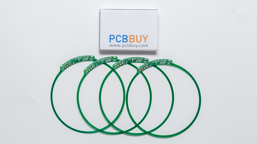
Printed Circuit Boards (PCBs) are fundamental components of electronic devices, and optimizing their production is crucial for cost efficiency and manufacturing speed. One key method for achieving this optimization is through PCB panelization, where multiple PCBs are fabricated in a single panel. This article provides an in-depth exploration of PCB panelization, offering seven critical tips that can enhance manufacturing efficiency, reduce waste, and ensure high-quality output.
Understanding PCB Panelization
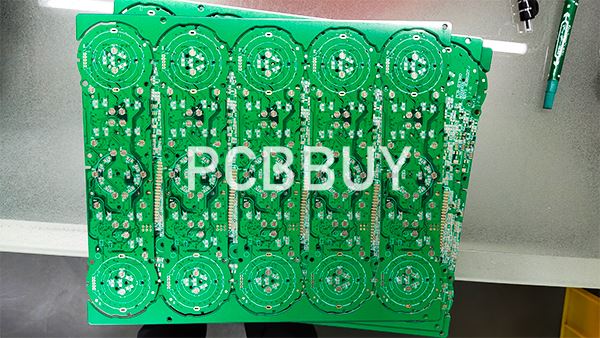
PCB Panelization is a process in which multiple individual PCBs are grouped into a single large board or panel. This technique allows manufacturers to handle, process, and manufacture several boards simultaneously, reducing the cost and time associated with individual PCB fabrication. The primary objectives of panelization include:
Minimizing Material Waste: By carefully arranging PCBs in a panel, manufacturers can maximize the use of the base material and minimize waste.
Reducing Production Costs: Handling multiple PCBs at once can significantly reduce the costs of production, including the time spent in processes like drilling, soldering, and surface finishing.
Improving Efficiency: Automated assembly and testing become more efficient when multiple PCBs are processed simultaneously.
Table 1: Benefits of PCB Panelization
|
Benefit |
Description |
|
Reduced Handling Time |
Fewer handling operations required per PCB. |
|
Material Efficiency |
Less material waste due to optimized panel layout. |
|
Increased Throughput |
More PCBs produced per batch. |
|
Cost Savings |
Lower cost per unit due to shared processing steps |
|
Easier Assembly |
Automated machines handle panels more effectively |
Tip 1: Optimize Panel Size
The size of the PCB panel is a crucial factor that influences manufacturing efficiency. Selecting the appropriate panel size requires balancing various factors:
Standard Panel Sizes: Most manufacturers use standard panel sizes, such as 18" x 24" (457 mm x 610 mm) or 20" x 26" (508 mm x 660 mm). Choosing standard sizes can reduce material costs and avoid custom tooling charges.
Machine Capabilities: Ensure that the panel size is compatible with the equipment used in manufacturing, such as pick-and-place machines, reflow ovens, and testing equipment. Oversized panels may not fit into standard machinery.
Material Utilization: Optimize the panel layout to minimize material waste. Use software tools to calculate the best arrangement of PCBs within a panel to maximize the use of the material.
Equation 1: Panel Utilization Efficiency

Where:
Total PCB Area is the combined area of all individual PCBs in the panel.
Total Panel Area is the area of the panel.
Tip 2: Choose the Right Panel Border
Panel borders are the spaces around the outer edge of the panel. They are crucial for handling, clamping, and aligning during the manufacturing process. Proper border design can prevent defects and ensure smooth processing.
Standard Border Width: A common border width is between 5 mm to 10 mm, depending on the manufacturing process and machinery.
Tooling Holes: Incorporate tooling holes in the panel border to ensure accurate alignment and registration during processing. These holes can also facilitate automated optical inspection (AOI).
Fiducial Marks: Place fiducial marks on the panel border to assist in the accurate placement of components by pick-and-place machines. Fiducial marks act as reference points for alignment.
Tip 3: Implement Breakaway Tabs and V-Grooves
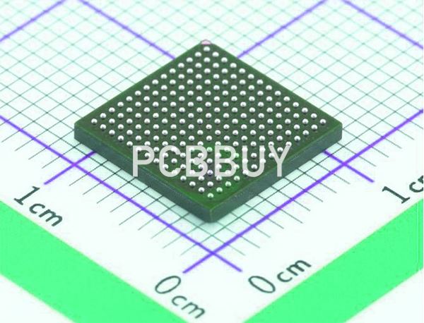
Breakaway tabs and V-grooves are methods used to separate individual PCBs from the panel after assembly. Selecting the appropriate method is critical for ensuring easy separation without damaging the PCBs.
Breakaway Tabs: These are small tabs that connect the PCB to the panel. They may include small holes (mouse bites) to facilitate easy breaking. Use breakaway tabs in areas that do not contain sensitive traces or components to avoid damage during separation.
V-Grooves: V-grooves are shallow cuts on both sides of the panel, allowing for easy snapping of the PCBs. This method is suitable for straight-line panelization and provides a clean separation.
Table 2: Comparison of Breakaway Tabs and V-Grooves
|
Feature |
Breakaway Tabs |
V-Grooves |
|
Suitable for |
Irregular or complex-shaped PCBs |
Straight-line PCBs |
|
Separation Method |
Manual breaking, possibly with pliers |
Snapping along the V-groove |
|
Impact on Board Edges |
May leave rough edges |
Generally cleaner edges |
|
Impact on Components |
Care needed near tab areas |
Less impact due to uniform separation |
Tip 4: Design Effective Tooling Holes
Tooling holes are used for mechanical alignment, positioning, and securing the PCB panel during manufacturing processes such as drilling, routing, and assembly.
Placement: Place tooling holes symmetrically to ensure balanced alignment. Typically, four tooling holes are placed near the corners of the panel.
Size and Shape: The size of the tooling holes should be standardized to match the pegs or fixtures used in the machinery. Circular holes are common, but specific equipment may require non-standard shapes.
Distance from Edges: Maintain a sufficient distance from the edges to avoid damage or misalignment. A typical distance is around 10 mm from the edge.
Tip 5: Use Proper Fiducial Marks
Fiducial marks are critical for accurate component placement and alignment, especially for surface-mount technology (SMT). Proper fiducial design ensures high precision in automated assembly.
Global Fiducials: Place at least three global fiducial marks on the panel to provide reference points for the entire panel. Ensure they are placed far apart, forming a triangle, to improve alignment accuracy.
Local Fiducials: Place local fiducials near complex components or areas requiring high precision. Local fiducials provide additional accuracy for specific sections of the PCB.
Shape and Size: Fiducial marks are usually circular with a contrasting background. A diameter of 1 mm to 2 mm is common, with a surrounding clearance area to ensure visibility.
Tip 6: Consider PCB Orientation
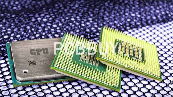
Proper orientation of PCBs within the panel can improve manufacturing efficiency and yield. Consider the following factors when orienting PCBs:
Uniform Orientation: Place all PCBs in the same orientation to simplify the assembly process, especially during component placement and soldering.
Heat Distribution: Optimize orientation to ensure even heat distribution during reflow soldering. This prevents hot spots and ensures consistent solder joints.
Component Placement: Align PCBs so that components with similar thermal requirements are grouped together. This allows for consistent processing conditions.
Equation 2: Optimal Orientation Calculation

Tip 7: Implement Panel Testing
Testing is a critical step in ensuring the quality of the PCBs before they are separated from the panel. Implementing in-panel testing can identify defects early, reducing waste and rework.
In-Circuit Testing (ICT): Design the panel with test points accessible to ICT probes. Ensure there is enough space around test points to accommodate probes without damaging the PCBs.
Flying Probe Testing: This non-contact testing method can be used for panels with fewer test points. Ensure that the test points are strategically placed for easy access.
Visual Inspection: Incorporate inspection windows or areas in the panel for automated optical inspection (AOI). Use these to check for defects like solder bridges, missing components, or alignment issues.
Conclusion
Effective PCB panelization is essential for optimizing manufacturing processes, reducing costs, and ensuring high-quality output. By following these seven tips—optimizing panel size, designing appropriate borders, using breakaway tabs and V-grooves, designing effective tooling holes, using proper fiducial marks, considering PCB orientation, and implementing panel testing—manufacturers can significantly improve their PCB production process. Proper panelization not only streamlines manufacturing but also enhances the reliability and performance of the final products.
References
1. IPC-2221: Generic Standard on Printed Board Design.
2. IPC-2222: Sectional Design Standard for Rigid Organic Printed Boards.
3. Lee, S. W. (2016). _PCB Design Techniques for Manufacturability_. McGraw-Hill Education.
4. Bosshart, W. (1991). _Printed Circuit Boards: Design and Technology_. Tata McGraw-Hill Education.
5. Montrose, M. I. (2004). _EMC and the Printed Circuit Board: Design, Theory, and Layout Made Simple_. IEEE Press.
Industry Category


