How to Make PCB Project for DIY Lover Step by Step?
By:PCBBUY 01/18/2022 09:34

When designing a circuit board it may sometimes seem as though arriving at the final design is going to be a long and arduous journey. Whether it’s the basics of micromanaging your copper and solder, or trying to ensure that your circuit board ends up printed after all, or going into more specific design problems such as through-hole technology or layout design with vias, pads, and any number of signal integrity issues, you’ll want to make sure you have the right design software.
If you are a DIY lover and you want to build a PCB project, please check and read the content below for more information.
How to design PCB Project?
Circuit board design and layout is both an art and a science, and it can be difficult to get started designing a new circuit board from scratch. If you’re new to electronics and circuit board design, and you’re still learning about designing a custom circuit board in Altium Designer®, we’ve compiled the 10 important steps you can use to create modern PCB layouts. In this tutorial, we'll show all the steps involved in creating your circuits and schematics, then we'll transition into creating a circuit board layout that can actually be manufactured.
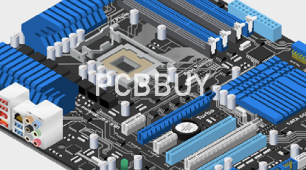
There is a lot that goes into any engineered design, from a basic printed circuit to a complex non rigid PCB. Any new electronic device will start as a block diagram and/or a set of electronics schematics. Once you have your schematics finished and validated, you can follow the steps below to create modern PCB layouts in Altium Designer. Here's the full list of PCB layout and design steps:
· Create the Schematic
· Create a Blank PCB Layout
· Schematic Capture: Linking to Your PCB
· Designing Your PCB Stackup
· Defining Design Rules and DFM Requirements
· Place Components
· Insert Drill Holes
· Route Traces
· Add Labels and Identifiers
· Generate Design Files
How to build a PCB Project?
You’ll need to use soldering equipment to solder the components to your PCB construction. If you are using a perfboard, single-sided PCB board, or double-sided PCB board, you’ll have to wire up all the components before you can test them. The best way is to put each component where you will mount it on your PCB project.
Check to see that everything fits, then test. If it all works, you are close to completion. It’s also a good idea to make sure that each of the components has a dedicated ground. You can solder them with the same color of solder that they are on your PCB project since green is the most common ground color for many components.

Double-side PCB boards can be hard to use if you don’t have access to the proper tools and equipment. You can get schematics of the circuit and components on the board, but you’ll need to add them to your PCB project layout. Many online services such as Hackaday, Oscillocast, and others offer free PCB layouts for DIY projects.
What are the characteristics of a good PCB design?
There are all sorts of things that go into the PCB design projects, but here are some of the most important characteristics.
It should be versatile enough to support many different types of applications
If you are building a custom circuit board, try to design it without limitations on one type of application. There may be reasons why you want to do this. Such as if you will sell the product in stores and need it to remain generic so that other people can use it for their applications or modifications. Consider the types of applications and plans you will use with your circuit or program and ensure they will work correctly
It should be easy to read, understand, and follow
When creating your PCB design, you can do many different things to make it rather complicated. Such as making it very detailed with lots of unique numbering and symbols for each component. Also, there can be a lot of space on the board not used for anything. Would you mind keeping all your PCB design in a way that makes them easy to follow? You can do it by using a simple numbering and symbol system and mostly using the space to make sense.
It should be easy to make changes to it when they are necessary
As you create your PCB design, you may find problems or areas of your project that you need to modify slightly. It doesn’t mean you have to start from scratch if they aren’t too complex
Industry Category


