How to Make PCB Stencil of Guidelines?
By:#PCBBUY 04/12/2022 10:14

Before you can go into production, solder paste is printed onto the component pads of the PCB. How can you make sure you apply the solder paste with precision exactly where it needs to go? Stencils, or formally surface mount technology stencils, are the answer. Stencils are the medium used to transfer that solder paste onto the PCB.
If you are going to learn more about the methods of making PCB stencil, please check and read the content below in this passage.
What is the basic definition of PCB stencil?
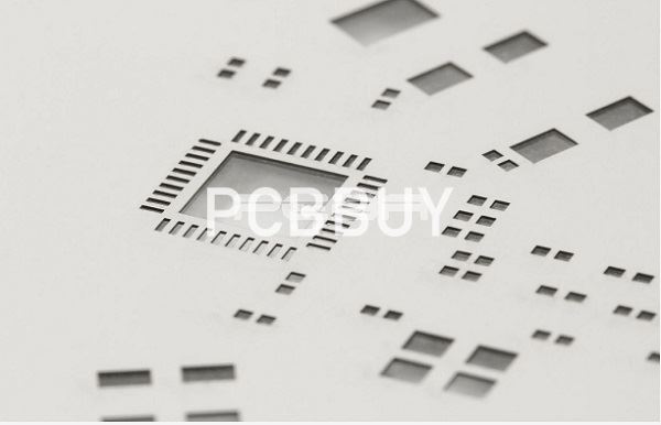
The sole purpose of an SMT stencil is to transfer solder paste to a bare circuit board. A stainless steel foil is laser cut creating an opening for every surface mount device on the board. Once the stencil is properly aligned on top of the board, solder paste is applied over the openings (making a single pass, using a metal squeegee blade). When the stainless steel foil is separated from the board, solder paste will remain, ready for placement of the SMD. This process, as opposed to hand soldering methods, ensures consistency and saves time.
What is the standard thickness of PCB stencil?
This is important to ensure there is good release of solder paste from the apertures and to obtain the correct volume of solder paste to achieve the desired solder joint. Typically the stencil thickness would be between 4 thou and 8 thou thick. If the stencil is too thick for the size of apertures then it can lead to the paste being held by surface tension to the inner walls of the aperture.
What are the types of PCB stencil?
The PCB stencil is utilized to store bind glue on assigned spots on an uncovered PCB board so that parts can be appropriately set and be entirely adjusted on the board. The fundamental feature and purpose of a PCB stencil are to precisely store the perfect measure of solder paste on SMT cushions for the weld joint between the cushion and the part to be appropriately structured concerning the electrical connection and mechanical strength. Utilizing a PCB Stencil to put solder paste makes the PCB Assembly process quicker and more efficient.
· Hybrid PCB Stencils
· Prototype or Photo PCB Stencils
· Frameless/ Reusable PCB Stencils
· Framed / Framework PCB Stencils
· Chemical-etch PCB Stencils
· Laser-cut PCB Stencils
What are the considerations of PCB stencil?
SMD-Stencils are precision tools which have to comply with high requirements, as they take a key role in the SMT (surface mount technology) process. We offer following SMD-Stencils:

Solder paste stencils are used to apply solder depots on printed circuit boards with a screen printing technique. SMD components (SMD = surface mounted device) are placed within these depots subsequently and soldered with a following reflow- or vapor phase process.
Stencils for adhesives are primarily used for mixed assembly, as substitution for a dispenser, and are necessary before component mounting and wave soldering.
Our lasered SMD-Stencils (made of stainless steel) allow a precise placement and strenght-of-shape of the solder- / adhesive- depots on the PCB and therefore accomodate the small track-widths and spacings as well as the hightech multipin components. Our SMD-Stencils are perfectly suited for finepitch and BGA assembly.
What are the requirements of PCB stencil?
The quality of the finished assembly is influenced by the SMD-Stencil used. The size of the apertures (openings), and thickness of the stencil determine the amount and shape of the applied paste.
The purpose of the SMD-Stencil is:
· Precise application of the needed material (solder paste, glue)
· Creation of depots defined in shape and size
· Reproducibility of the print
· Effective cleaning of the pads
· Economy
To ensure an optimum result for the production of your SMD-Stencils, please note the following design hints.

What is the data of PCB stencil?
Data Format Regardless of the SMT stencil fabrication method used, Gerber data is the preferred data format. There are two standard Gerber formats available:
· RS-274D – requires a data file listing the X-Y coordinates on the SMD stencil where apertures are to be placed and formed, and a separate Gerber aperture list that describes the size and shape of the various Gerber apertures used to prepare the image.
· RS-274X – in this format the Gerber aperture list is embedded in the data file.
Industry Category


