How to Make Vias in PCB through 7 Effective Methods for Beginners?
By:PCBBUY 10/29/2021 09:22

Vias are vital in multi-layered boards, which are challenging to design and produce. They create routes for the sufficient flow of electrical and thermal current between the board's different layers. In brief, vias are basically channels that vary in size and type.
Are you a beginner for PCB manufacturing? If you are interested in the methods of making PCB vias, please check and read the content for more professional knowledge.
If you want to order PCB product, please check and custom your order online.
1. How to route high-speed signal vias on PCB?
Like signal traces, vias introduce inductance and capacitance to the circuit. In signals with lower frequencies, such characteristics are often negligible. However, placing vias on high-speed traces can alter the impedance and affect signal integrity. It’s advisable to avoid using vias on high-speed signals.
2. How to pay attention to signal degradation of PCB via?
You’ll also need to be wary of via stub, where a portion of the drilled via is unused. Via stubs exist when signals are routed from an outer layer to the middle layer, leaving the remaining section acting as an antenna. Via stubs may degrade the signal traveling on the trace itself. To prevent via stubs, back drilling is performed to remove the unused copper section on the via.
3. How to plate vias on PCB?
It is often desirable to perform additional treatments to the vias later in the production sequence to improve either thermal performance or assembly yield. These may include epoxy hole filling, secondary solder masking, or some combination of the two.
These additional process steps are most often intended to eliminate assembly issues such as solder shorting between a component pad to a via pad or solder migrating down through the barrel of a via which has been drilled into a component soldering land. These problems lead to costly troubleshooting and rework. Fortunately, it is possible to eliminate most issues by specifying an appropriate via treatment.
Tented vias have a non-conductive solder mask covering over the pad at both ends of the hole. Tenting was popular when dry film solder mask was in its prime, because dry film’s 0.004” thickness enabled it to tent even relatively large holes very reliably without much chance of breakdown. Today however, dry film mask is no longer used since its height causes difficulty with modern surface mount soldering.
4. What are the limitations for multilayer PCB?
Underwriter laboratories say that for supreme quality and reliability, you should not produce PCBs that need over three lamination steps. It means that you should not design vias such that they need more than three steps for assembly. This issue arises when you are dealing with PCBs having more than six layers.
Figure 4 shows an example of a 10-layer PCB that would need two lamination steps. The first step, drill the buried holes and electroplate them from layers 3 to 8. In the second step, drill the blind holes and electroplate them on their layers and then laminate the rest of the layers. In the end, drill the through-hole vias and electroplate them, but this is not a lamination step. Hence, this PCB board only requires two lamination steps and three drilling steps.
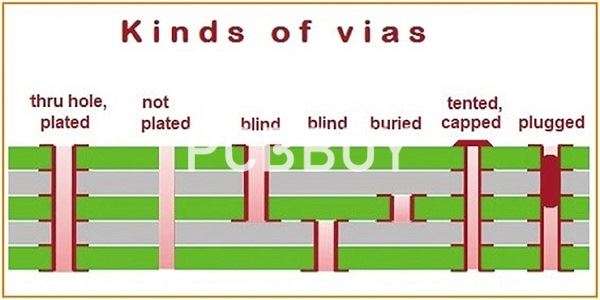
5. What are the 5 types of PCB via?
Via
A plated-through hole(PTH) for inner layer connection and not for inserting component leads or other reinforcing materials.
Blind via
The hole does not pass through the entire workpiece. The blind hole always has a specified depth, which usually does not exceed a certain ratio (aperture). The literal meaning of a “blind hole” is that it is not possible to see through the hole. For example, for a 6-layer board, the drilling is only from layer 1 to layer 4. This is called a blind hole.
Buried via
Buried Via is a copper-plated hole that connects two or more internal layers of the board and is not accessible by the external layers. And it’s not possible to discover a buried viain a PCB because it is “buried” under the external layer surfaces of the board. For example, for a 6-layer board, the drilling only goes from layer 3 to layer 4; this is called buried via.
Though via
The through-holes extend from one outer layer of the PCB to another outer layer.
Component hole
They are holes for fixing the components on the printed board and electrically connecting the conductive patterns.
6. How to select vias for PCB?
In ordinary PCB design, the parasitic capacitance and parasitic inductance of the via have little effect on the PCB design. For 1 to 4 layer PCB design, it is better to use 0.36mm/0.61mm/1.02mm (drilled hole/pad/power isolation area) via holes.
Some signal wires with special requirements, such as power wires, ground wires, clock wires, etc., can choose 0.41mm/0.81mm/1.32mm hole. They can also choose other sizes of holes according to the actual conditions.
7. What are the benefits of PCB via?
Because PCBs have limited amounts of space, blind and buried vias can be a huge benefit. They allow you to keep the PCB small, which is essential when working with electronics. The use of vias frees up space on the surface of the board; that space can then be used for other functions. Vias are a relatively simple solution, but you will need to be aware that the addition of blind and buried vias will add to the cost of the board.
Because there are many factors that go into getting the right PCBs with the correct blind and buried vias, it is important to work with a quality manufacturer.
Industry Category


