How to Manufacture PCB with 5 PCB Plating Techniques?
By:PCBBUY 10/09/2021 09:21

When the topic of circuit board plating is discussed, it is immediately assumed that a multilayer PCB, which may have various via types, is the focus. Although it certainly could be, this is too narrow a perspective. A more comprehensive definition of PCB plating is given in the content below.
In this passage, you could learn everything about the PCB plating techniques during the manufacturing process. Check and read the content we provide to learn more professional information PCB plating techniques
What are the preparations in PCB plating process?
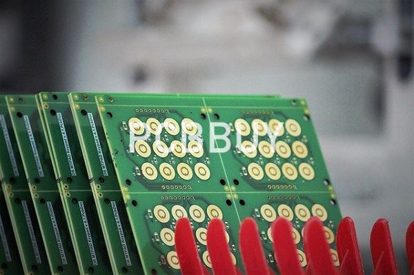
The first PCB plating process will be an electroless procedure that will chemically coat a thin layer of copper to the board’s surface areas, including the drilled holes’ interior. This plating operation aims to create a thin metal base on the board and in the holes that will serve as the foundation for the electroplating process. Next, the board will be prepared for electroplating:
· The holes are cleaned of contaminants and residues from drilling.
· The holes’ interior is prepped with a micro etching to help the copper binding.
· Both the top and the bottom of the board are covered with a photoresist material.
· The photoresist is exposed to ultraviolet light except for where the metal circuitry patterns are to be plated.
· The pliable photoresist covering the circuitry patterns is washed off, leaving the rest of the board surface areas masked by the hardened photoresist.
What are the 5 PCB plating techniques during manufacturing process?
1. What is HASL?
HASL is the alias name of hot air solder leveling. So, it’s a reliable copper PCB plating. Plus, you can produce it by plunging the board in a solder. Also, this solder mask must be molten. Hence, you can level the plating with a hot air knife.
The surface is not completely level, so this can cause issues with small components. The solder used is typically Tin-Lead. That means that it isn’t RoHS compliant. And if reducing the amount of lead you use is important, you may want to choose Lead-Free HASL instead.
HASL Advantages:
· Excellent solderability
· Inexpensive / Low cost
· Allows large processing window
· Long industry experience / well-known finish
2. What is Immersion Tin?
Immersion Tin is a metallic coating of ‘Tin’, which is deposited directly over the top copper layer of a PCB using an electroless chemical bath process. PCB finishes are used to protect the copper tracks and pads on printed circuit boards while in storage. Immersion Tin forms a dense uniform coating with good hole wall lubricity. Its appearance is usually White, so it is also called ‘White Tin’.

Advantages of Immersion Tin:
· Shelf-life: 6 months
· Easy to rework (but rework should be limited)
· Due to its planarity (flatness), suitable for fine-pitch/ BGA/ small components placement
· Not expensive
· Good for backplane panels, which are assembled using press fit pin insertion
· Offers good solderability after exposure to various thermal cycles
3. What is ENIG?
ENIG (Electroless Nickel Immersion Gold) is a surface plating that is applied over the copper pads on a Printed Circuit Board to protect them from corrosion and other abnormalities. Initially, the copper pad is covered by a Nickel (Ni) layer followed by a thin immersion Gold (Au) layer. ENIG provides good oxidation resistance, excellent surface planarity and allows for easy soldering which results in excellent electrical performance of the PCB board.
Advantages of ENIG Surface Finishes:
· It provides impressive wettability, surface planarity, coplanarity, and long shelf life to the PCB board since immersion gold has strong chemical properties.
· In ENIG, the nickel layer acts as a barrier and stops the interfusion between gold and copper. It also produces an IMC Ni3Sn4 to provide good solderability after reacting with Tin.
· Low contact resistance, high strength, reduces oxidation, and provides antifriction.
· It provides good plating over the copper pads and via holes.
· Its excellent surface planarity allows the components to be soldered flat onto the pad, making it ideal for BGA pads and other fine-pitch components.
· ENIG complies with all RoHS requirements.
4. What is Immersion Silver?
This surface PCB plating process refers to the creation of a thin silver layer over a copper layer. In other words, it involves the immersion of copper objects into a silver ion solution.

So, many engineers in the electronics sector use the immersion silver plating process. Plus, they use it during PCB production—to stop copper conductors from oxidizing.
5. What is Electroplating?
The Electroplating procedure involves the use of DC. Plus, this DC helps to produce a chemical process that deposits metal plates over copper objects. In this case, the metal can be nickel, tin, or even gold. Generally, this method is ideal for through-hole vias and surface traces.
Industry Category


