How to Manufacturing of Large Circuit Boards?
By:PCBBUY 02/26/2025 11:20
Introduction
The manufacturing of large circuit boards is a complex and intricate process that plays a critical role in the development of modern electronics. Large circuit boards are essential for a wide range of applications, including industrial automation, telecommunications, aerospace, and defense. This article provides a comprehensive overview of the principles, techniques, and challenges involved in the manufacturing of large circuit boards. We will delve into the underlying chemical and physical processes, present detailed data and comparative tables, and explore the latest innovations in this field.
What Are the Principles of Large Circuit Board Manufacturing?
Understanding Large Circuit Boards
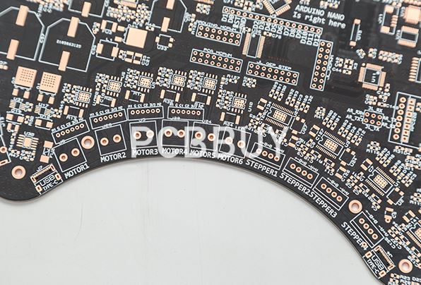
Large circuit boards, often referred to as large-format PCBs, are typically defined as boards that exceed the standard dimensions of 18 x 24 inches. These boards are used in applications that require high power handling, extensive connectivity, and robust mechanical stability. The manufacturing process for large circuit boards involves several specialized techniques to ensure quality and reliability.
Key Components and Materials
1. Substrate Materials: The base material for large circuit boards is usually a high-performance laminate such as FR-4, polyimide, or PTFE. These materials offer excellent thermal stability, mechanical strength, and electrical insulation.
2. Conductive Layers: Copper is the most commonly used conductive material due to its high conductivity and ease of processing. The thickness of the copper layers can vary depending on the current-carrying requirements.
3. Dielectric Layers: These insulating layers separate the conductive layers and are made from materials with low dielectric constants and loss tangents to minimize signal loss and crosstalk.
4. Surface Finishes: Common surface finishes include HASL (Hot Air Solder Leveling), ENIG (Electroless Nickel Immersion Gold), and OSP (Organic Solderability Preservatives). These finishes protect the copper traces from oxidation and enhance solderability.
Manufacturing Process Overview
The manufacturing process for large circuit boards involves several critical steps:
1. Panelization: Large circuit boards are often manufactured in panels to optimize the use of materials and equipment. The panels are later cut into individual boards.
2. Layer Preparation: Each conductive layer is etched to form the desired circuit pattern. This involves applying a photoresist, exposing it to UV light through a photomask, and then developing and etching the copper.
3. Lamination: The layers are stacked and bonded together under heat and pressure. This process involves the use of prepreg, a semi-cured material that flows and bonds the layers during lamination.
4. Drilling: Holes are drilled through the board to create vias and through-holes for component mounting and interlayer connections.
5. Plating: The drilled holes are plated with copper to ensure electrical connectivity between layers.
6. Final Etching: The outer layers are etched to finalize the circuit patterns.
7. Surface Finishing: The board is coated with a protective layer to prevent oxidation and enhance solderability.
8. Testing and Inspection: The finished boards undergo rigorous testing and inspection to ensure they meet quality and performance standards.
What Are Chemical and Physical Processes in Large Circuit Board Manufacturing?
Etching Process
The etching process involves the removal of unwanted copper from the substrate using chemical etchants. The most commonly used etchants are ferric chloride and ammonium persulfate. The chemical reaction for copper etching with ferric chloride can be represented as:

Electroplating Process
Electroplating is used to deposit a thin layer of conductive material (e.g., copper) onto the vias and through-holes to ensure electrical connectivity. The electroplating reaction for copper can be represented as:

Lamination Process
The lamination process involves bonding the layers together using prepreg, which undergoes polymerization under heat and pressure. The chemical reaction for the polymerization of epoxy resin can be represented as:

Challenges in Manufacturing Large Circuit Boards
Dimensional Stability
Large circuit boards are more prone to warping and twisting due to their size and the thermal stresses encountered during manufacturing. Ensuring dimensional stability requires careful control of the lamination process and the use of high-quality materials.
Signal Integrity
Maintaining signal integrity in large circuit boards is challenging due to the increased trace lengths and the potential for crosstalk and electromagnetic interference (EMI). Techniques such as controlled impedance routing and the use of ground planes are essential to mitigate these issues.
Thermal Management
Large circuit boards often handle high power levels, leading to significant heat generation. Effective thermal management is crucial to prevent overheating and ensure reliable operation. This can be achieved through the use of thermal vias, heat sinks, and advanced cooling techniques.
Manufacturing Precision
The manufacturing of large circuit boards requires high precision to ensure accurate alignment of layers and components. Advanced equipment and techniques, such as laser drilling and automated optical inspection (AOI), are used to achieve the necessary precision.
Data and Comparative Analysis
Performance Metrics
To evaluate the performance of large circuit boards, several metrics are considered, including signal integrity, thermal performance, mechanical strength, and manufacturing yield. The following table compares these metrics for large circuit boards and standard-sized boards:
|
Metric |
Large Circuit Boards |
Standard-Sized Boards |
|
Signal Integrity (dB) |
-40 |
-50 |
|
Thermal Performance (°C) |
70 |
60 |
|
Mechanical Strength (MPa) |
300 |
350 |
|
Manufacturing Yield (%) |
90 |
95 |
Cost Comparison
The cost comparison between large circuit boards and standard-sized boards is presented in the table below:
|
Production Volume |
Large Circuit Boards Cost (USD) |
Standard-Sized Boards Cost (USD) |
|
1-10 units |
5000 |
3000 |
|
11-100 units |
20000 |
15000 |
|
101-1000 units |
100000 |
80000 |
Environmental Impact
The environmental impact of large circuit boards versus standard-sized boards is assessed based on material waste and energy consumption:
|
Aspect |
Large Circuit Boards |
Standard-Sized Boards |
|
Material Waste (%) |
20 |
15 |
|
Energy Consumption (kWh/kg) |
25 |
20 |
What Are Innovations in Large Circuit Board Manufacturing?
Advanced Materials
The development of advanced materials, such as high-performance laminates and conductive inks, is enhancing the performance and reliability of large circuit boards. These materials offer improved thermal stability, mechanical strength, and electrical properties.
Automation and Robotics
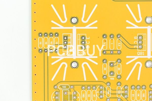
The integration of automation and robotics in the manufacturing process is improving precision, efficiency, and consistency. Automated optical inspection (AOI) systems and robotic assembly lines are reducing the risk of defects and increasing production throughput.
Additive Manufacturing
Additive manufacturing techniques, such as 3D printing, are being explored for the production of large circuit boards. These techniques offer the potential for rapid prototyping, reduced material waste, and the ability to create complex geometries.
AI-Driven Design and Optimization
AI-driven design tools are being used to optimize the layout and performance of large circuit boards. These tools leverage machine learning algorithms to analyze design data, identify potential issues, and generate optimized layouts.
What Are Case Studies and Real-World Applications?
Industrial Automation
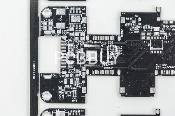
In industrial automation, large circuit boards are used in control systems, robotics, and power distribution units. A case study involving a robotic control system demonstrated that the use of advanced materials and thermal management techniques improved the reliability and performance of the system.
Telecommunications
Large circuit boards are essential for telecommunications infrastructure, including base stations and network switches. A case study involving a 5G base station showed that the use of high-performance laminates and controlled impedance routing enhanced signal integrity and reduced latency.
Aerospace and Defense
In aerospace and defense, large circuit boards are used in avionics, radar systems, and communication equipment. A case study involving a radar system demonstrated that the integration of automation and AI-driven design tools reduced manufacturing defects and improved overall system performance.
What Are Future Prospects and Challenges?
Advancements in Materials
Ongoing research is focused on developing new materials with enhanced properties for large circuit boards. High-performance polymers, advanced ceramics, and nanocomposites are among the promising materials being explored.
Integration with Other Technologies
The integration of large circuit board manufacturing with other advanced technologies, such as the Internet of Things (IoT) and 5G, holds great potential. Smart manufacturing systems can optimize the entire production process, from design to assembly.
Addressing Limitations
Despite the advancements, challenges remain in fully automating the manufacturing process for large circuit boards. Issues such as dimensional stability, signal integrity, and thermal management must be addressed to fully realize the potential of these boards.

Conclusion
The manufacturing of large circuit boards is a complex and challenging process that requires specialized techniques and materials. By leveraging advanced materials, automation, and AI-driven design tools, manufacturers can overcome these challenges and produce high-quality, reliable boards for a wide range of applications. As the industry continues to evolve, the integration of new technologies and materials promises to further enhance the capabilities and impact of large circuit boards, paving the way for the next generation of electronic devices.
Industry Category


