How to Meet the Requirements of PCB Layout Preparation?
By:PCBBUY 08/24/2024 16:23

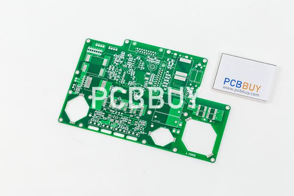
Printed Circuit Board (PCB) design is a critical part of electronic product development. The layout of a PCB determines how components are arranged, how signals are routed, and how the board interfaces with the outside world. Ensuring that the PCB layout meets the required specifications is essential for functionality, reliability, and manufacturability. This article will explore how to meet the requirements of PCB layout preparation, discussing key principles, guidelines, and techniques.
1. Understanding PCB Layout Basics
Before diving into the specific requirements, it's important to understand the basics of PCB layout:
Components Placement: The physical arrangement of components on the board is the first step in PCB layout. Components should be placed logically, considering their functions, connections, and potential heat generation.
Signal Routing: After placing the components, the next step is routing the signal traces. These traces connect different components on the PCB, and their layout can significantly affect the performance of the circuit.
Power and Ground Planes: Efficient power distribution and proper grounding are crucial for maintaining signal integrity and reducing noise.
Via Usage: Vias are used to connect different layers of a PCB. Their placement and size must be carefully considered to ensure reliable connections without introducing unwanted parasitics.

2. Design Rule Check (DRC) and Electrical Rule Check (ERC)
Design Rule Check (DRC) and Electrical Rule Check (ERC) are automated verification processes used to ensure the layout meets specific manufacturing and electrical standards.
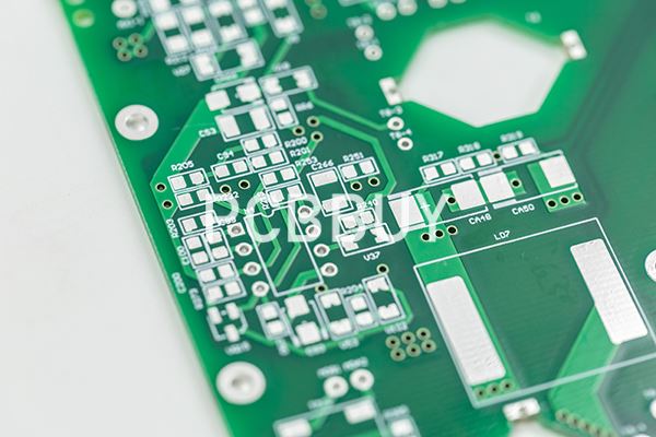
DRC ensures that the physical layout adheres to the manufacturing constraints, such as minimum trace width, spacing between traces, and via size.
ERC checks for electrical issues like unconnected pins, net short circuits, and potential signal integrity problems.
Table 1: Common DRC Parameters
|
Parameter |
Description |
Typical Value |
|
Minimum Trace Width |
The smallest width of any signal trace |
5 mils (0.127 mm) |
|
Minimum Trace Spacing |
The smallest distance between two traces |
5 mils (0.127 mm) |
|
Minimum Via Diameter |
The smallest diameter of a via |
10 mils (0.254 mm) |
3. Signal Integrity Considerations
Signal integrity issues, such as reflection, crosstalk, and electromagnetic interference (EMI), can degrade the performance of high-speed PCBs. Meeting the requirements of signal integrity involves:
Controlled Impedance Traces: Ensure traces carrying high-speed signals have controlled impedance to prevent signal reflection. The impedance \( Z_0 \) of a trace can be calculated using:


Differential Pairs: For signals like USB, HDMI, and Ethernet, use differential pairs. Ensure the traces in a differential pair are of equal length to maintain signal integrity.
Crosstalk Mitigation: To minimize crosstalk, maintain adequate spacing between high-speed traces and use ground planes effectively.
4. Thermal Management
Thermal management is a critical aspect of PCB design, especially for boards that handle high currents or house heat-generating components like processors and power regulators.
Thermal Vias: Use thermal vias to dissipate heat from the top layer to the inner or bottom layers. The number and placement of thermal vias depend on the heat dissipation requirement.
Heat Sinks and Copper Pour Incorporate heat sinks where necessary and use copper pour areas to spread and dissipate heat. Calculate the thermal resistance of the PCB using:

5. Grounding and Power Distribution
Proper grounding and power distribution are essential to prevent noise and ensure the stable operation of electronic circuits.
Ground Plane Design: Use a solid ground plane to provide a low impedance path for return currents. Avoid cutting the ground plane with traces or slots, as it can create ground loops and increase EMI.
Decoupling Capacitors: Place decoupling capacitors near power pins of ICs to filter out noise. The placement and value of these capacitors should be chosen based on the frequency range of the noise.
Power Plane: Use a dedicated power plane for high-current circuits to ensure stable voltage levels. The power plane should be adjacent to the ground plane to reduce impedance.
6. Design for Manufacturability (DFM)
Designing a PCB that is easy to manufacture can reduce costs and improve yield. Key considerations include:
Panelization: Arrange multiple PCBs in a panel to optimize material usage and reduce handling time. The panel design should consider the routing paths and tooling holes for easy processing.
Component Placement and Orientation: Place components with similar orientations to facilitate automated pick-and-place assembly. Avoid placing components too close to the edge of the PCB to prevent damage during handling.
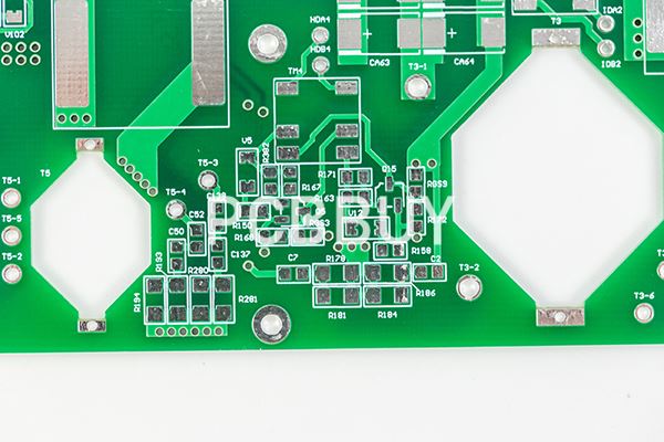
Solder Mask and Silkscreen: Ensure that the solder mask openings align with the pads, and there is sufficient clearance between silkscreen markings and pads to avoid issues during soldering.
7. Simulation and Prototyping
Before finalizing the PCB layout, it's crucial to simulate and prototype the design:
Simulation Tools: Use tools like SPICE, HyperLynx, and ANSYS to simulate signal integrity, thermal behavior, and electromagnetic compatibility (EMC).
Prototyping: Create a prototype to test the actual performance of the PCB. This step helps identify issues that may not be apparent in simulations and allows for adjustments before mass production.
8. Compliance with Standards
Meeting industry standards ensures the reliability and safety of the PCB. Key standards include:
IPC-2221: General standard for PCB design, covering materials, design techniques, and testing.
IPC-6012: Qualification and performance specification for rigid PCBs.
IEC 61010-1: Safety requirements for electrical equipment, ensuring safe operation under specified conditions.
Conclusion
Meeting the requirements of PCB layout preparation involves a careful balance of electrical, thermal, and mechanical considerations. By understanding the fundamentals, adhering to design rules, and leveraging advanced simulation tools, engineers can create PCBs that meet performance, reliability, and manufacturability standards. Following these guidelines not only ensures a successful PCB design but also reduces the likelihood of costly revisions and delays in production.
References
1. IPC-2221: Generic Standard on Printed Board Design.
2. IPC-6012: Qualification and Performance Specification for Rigid Printed Boards.
3. Boysen, E., & Durkop, M. (2015). _PCB Design for Real-World EMI Control_. Kluwer Academic Publishers.
4. Howard Johnson, Martin Graham. (2003). _High-Speed Digital Design: A Handbook of Black Magic_. Prentice Hall PTR.
5. Montrose, M. I. (2000). _EMC and the Printed Circuit Board: Design, Theory, and Layout Made Simple_. IEEE Press.
Industry Category


