How to Operate PCB before Laminating Chemical Copper Surface Treatment?
By:PCBBUY 04/30/2025 16:57
The chemical method is characterized by the use of traditional chemical reagents in its process, and it is mostly carried out in aqueous solution, which belongs to the category of wet process. Chemical methods mainly include chemical micro-etching technology, blackening technology, brown technology, and bleaching technology.
What is Chemical Micro Etching?
Overview of chemical micro etching technology
Chemical micro etching technology is the use of chemical action on the copper surface or substrate of the printed circuit board to implement corrosion (oxidation or degradation), reaction or dissolution of surface micro-areas, forming microscopic pits or active sites, to improve the surface performance of the printed circuit board, enhance the interlayer bonding force and product electrical performance and other goals.
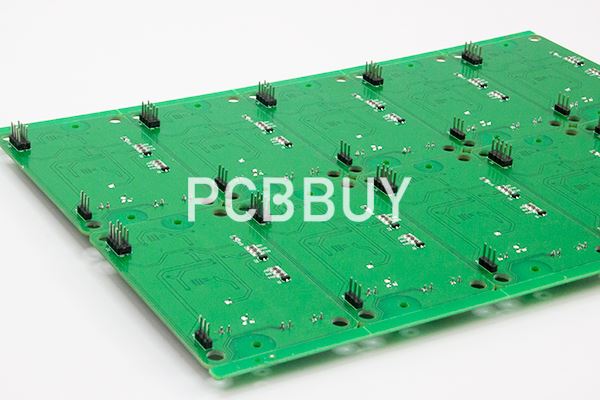
In the manufacture of multi-layer printed circuit board, chemical micro-etching technology plays a very important role in the production of inner layer, micro-etching rough, bright surface is conducive to the improvement of mechanical and chemical bonding force, so that dry film and circuit board surface fit. Main uses of chemical micro etching liquid:
Pretreatment of tin spray;
Pretreatment of coating heat-resistant water-soluble copper protection agent;
Pre-treatment of printed anti-weld edge paint;
Pre-treatment of dry film pressing such as inner layer and outer layer;
Pre-treatment of single panel coating rosin;
Copper surface treatment of carbon ink printed board and silver glue perforated board.
Basic principle of chemical micro etching technology
The chemical composition of copper foil is relatively inert copper elemental substance. According to the basic principle of chemistry, the reagent used to dissolve it is a strong oxidizing system with strong corrosion, such as copper chloride-hydrogen peroxide aqueous solution system. The oxidizer of these etching liquid reacts with copper to dissolve the copper surface in the micro zone, thus forming a convex and concave surface to enhance the interlayer bonding force of multi-layer board, improve the thermal stability of the product to prevent the appearance of explosive board. The chemical nature of different etching systems is the same, and the difference lies in the specific reaction details.
The research shows that the direction and rate of chemical reaction will directly affect the quality of chemical microetching. In the actual production, people generally pay attention to the following factors: the formula of the etching liquid system, the temperature of the implementation system, the accumulation of copper ions in the etching.
What is Blackening Technology?
Overview of blackening technology
In the production process of multi-layer printed circuit board, due to the inconsistent coefficient of thermal expansion of copper foil and resin, the two binding forces are not enough when heated, and it is easy to layer at the interface, and the surface treatment of copper performance is required before laminating, and blackening technology is one of the treatment technologies.
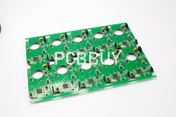
The blackening technology of copper foil in printed circuit board is a kind of inner layer treatment technology of printed circuit board before lamination developed on the basis of chemical micro etching technology.
The purpose of blackening technology:
(1) Increase the specific surface area of the copper foil, thereby increasing the contact area with the resin, which is conducive to the full diffusion of the resin, and the flowing resin can be embedded in these surface layers during lamination to form a larger binding force.
(2) The non-polar copper surface is transformed into a polar and surface, and the binding force between the copper surface and the resin polar bond is increased.
(3) The surface is not affected by moisture at high temperatures, reducing the possibility of copper and resin separation.
The blackening effect is affected by many factors. Process parameters such as PH value, oxidizer concentration, treatment temperature and time of blackening solution are affected.
With the increase of oxidizing agent concentration, the growth rate of the blackened layer increases, and the peel strength of the copper foil increases first and then decreases. The reason is that the crystal structure of the copper foil after oxidation is directly related to the peel strength, and the crystal particles are small and uniform, which produces a large binding force with the resin. With the increase of the morphology of crystalline particles, the surface area decreases and the peel strength decreases naturally. If the process parameters are not properly controlled, the possibility of pink circle is greater. The so-called pink ring refers to the junction between the hole wall and the inner hole ring, and the oxide film on the copper surface of the hole ring has been discolored, or due to chemical reactions, it has been exposed to the natural color of copper (pink). Pink rings are usually found in the late production of the printed circuit board, which directly affects the quality pass rate of the multi-layer board.
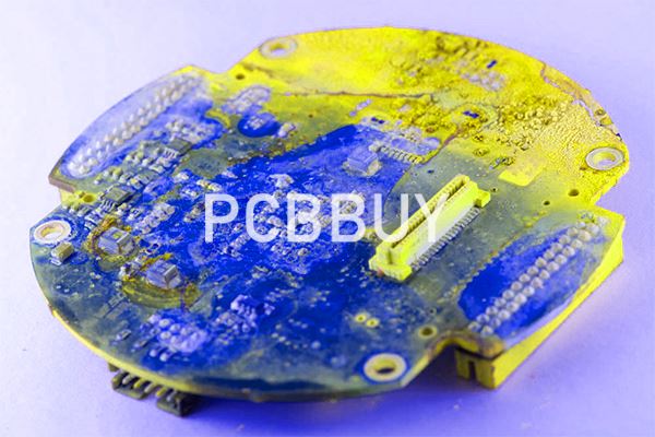
In the printed board production process, the inner layer surface treatment, lamination, curing, drilling, etching, chemical copper deposition, copper plating and other processes may lead to the production of pink rings, the key is whether the blackening layer and the substrate is firmly combined and the blackening layer corrosion resistance is strong. Printed board in the production process to withstand the vertical mechanical impact and horizontal chemical erosion force, the layer should have enough adhesion to resist these two harmful effects, the layer resistance to peel strength is low and black layer corrosion resistance is poor is the main reason for pink ring.
Basic Principles of blackening technology
The oxidation reaction between copper foil and oxidant in blackening solution is the main reaction of blackening technology. Through the reaction, a uniform, dense and reasonably long needle-like oxidation crystal layer is formed on copper surface, and its appearance is needle-like villi layer. The honeycomb loose structure formed after reduction increases the specific surface area of the copper surface, reacts with semi-solid lamination at high temperature in the lamination stage, and enhances the adhesion between the copper surface and the semi-cured resin.
Formulations and functions of common blackening agents
|
No. |
Constituent |
Effect |
|
1 |
NaCIO2 |
Oxidizing agent |
|
2 |
NaOH |
Provide an alkaline environment |
|
3 |
Na2CO3 |
Buffer, adjust pH |
|
4 |
Na3 CO4 |
Buffer, adjust pH |
|
5 |
Organic additive |
Crystal refiner to improve surface uniformity |
Some cuprous oxide and copper, which are not easy to react with acid, are generated in the blackened layer through the reaction, so that the reduced oxide layer has a certain ability to resist dilute acid attack, thus effectively reducing the generation of pink rings. However, after blackening the copper surface, the black acicular crystal structure composed of cuprous oxide and cuprous oxide on the surface is vulnerable to acid chemical attack. There are several problems with this process that are difficult to overcome.
(1) Short circuit problem: the texture of the black layer needle-like crystal is brittle, and too long crystals are easy to break, if the broken crystals remain between the lines, it will cause short circuit or ion migration and other problems, thereby reducing the reliability of insulation between the lines.
(2) Blackening to obtain CuO layer thickness control problem. If the thickness of the black CuO layer is too large, the dendritic structure formed is easy to break, resulting in the formation of copper, resin interface than the binding force is even worse than before treatment.
(3) Limited material selection: The blackening technology uses a strong alkaline treatment solution, and it is difficult to use this method for resin materials with low alkaline resistance.
(4) The blackening technology has a long process, high required temperature, and difficult sewage treatment.
Blackening technology process flow
Alkaline oil removal -- "micro-corrosion --" sulfuric acid pickling -- "pre-leaching --" oxidation -- "post-leaching, etc.
What is Browning Technology?
Overview of Browning technology
In the process of manufacturing multi-layer printed circuit boards, in order to enhance the interlayer bonding force between the inner layers, researchers have carried out various explorations, and blackening technology is one of the successful cases. The defects of blackening technology itself, such as the occurrence of pink circles, high temperature operation, complex process, long operation time, the need to use dangerous materials, etc., and these defects have been difficult to avoid through technical improvement, and have become the original driving force for the industry to find new processes to replace blackening technology.
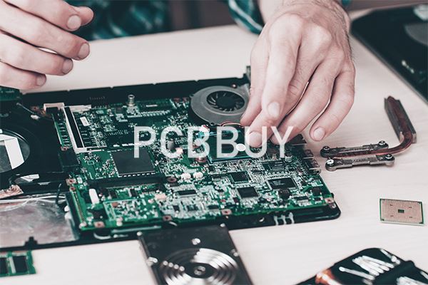
Basic consensus of brown chemical technology industry: Using the principle of REDOX and metal ion complexation, the surface of copper is treated in a specific liquid system. After certain chemical action, a layer of organic metal compound with uniform and good bonding properties is generated on the surface of copper, and the surface of copper layer is coarsed-controlled before the inner layer is bonded. A surface treatment metal technique that enhances the bonding strength between the inner copper layer and the semi-cured sheet after pressing the board.
The brown treatment of copper surface wets the inner copper surface, enhances the bonding force between the semi-cured sheet (PP) and Cu, and prevents the "burst board" stratification due to poor bonding force. The Browning process is the oxidation reaction of copper in the acidic medium, the main product is cuprous oxide, etc. Its structure is tight and non-porous, and the adhesion with the semi-cured sheet is far greater than the black layer. In addition, the cuprous oxide film is dense, complete, uniform, and can provide a consistent roughness, which provides a good physical structure for the next organic metal conversion film.
Browning mechanism
In the manufacture of high-quality multilayer printed circuit boards, the main factors determining the binding force between copper foil and resin are:
(1) The way and degree of copper foil surface coarsening
(2) Type and thickness of organic oxide film on copper foil surface
Brown technology is around the two factors, through the treatment of copper surface to improve the quality characteristics of printed circuit boards.
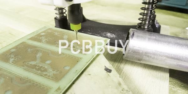
The essence of the brown treatment technology is a chemical method, and the brown solution is mainly composed of sulfuric acid, hydrogen peroxide and specific organic matter. In the process of treatment, the hydrogen peroxide in the brown solution oxidizes Cu to form copper oxide and heterocyclic organic compounds containing N, O, S, etc. Under the joint action of adhesive and plasticizer, an organometallic film with rough appearance of honeycomb is formed on the surface of copper. In the lamination process, the curing gumming reaction with resin occurs, and the binding force and heat resistance of copper and resin are improved. Therefore, the binding force between copper foil and resin after Browning mainly comes from two aspects:
(1) Increase the contact surface area between copper and resin
(2) The formation of a layer of organic metal conversion film, the conversion film can achieve chemical bonding with the resin layer, so as to obtain a higher binding force than the physical adsorption, while the conversion film can also maintain the stability of the organic metal film itself, improve its acid resistance, prevent further corrosion of copper, so as to protect the line graphics, to ensure the quality and reliability of multi-layer printed circuit board.
Browning process flow
Process flow: the previous process -- "two countercurrent washing --" oil removal -- "water washing --" prepreg -- "Brown --" water washing -- "deionized water washing --" blow dry -- "board --" Drying board -- "the next process
Defects and challenges of Browning process
(1) The challenges of lead-free process of printed circuit board manufacturing:
The lead-free welding temperature is 30 degrees higher than the eutectic temperature of traditional lead tin, reaching 260 degrees, and the heat absorption of printed circuit boards is greatly increased, and the heat resistance of printed circuit boards must be improved to match with it.
(2) The challenge of high-frequency signal transmission of electronic products:
In addition to the continuous development of high density, multi-function and high reliability of today's electronic products, the most prominent problem is the high frequency and high digitalization of signal transmission. High frequency digitized signal. The transmission of high frequency or high digital signals in PCB wires mainly brings the following problems: the skin effect of high frequency. Because the skin effect caused by high-frequency is more and more serious, the transmission signal loss is more and more serious.
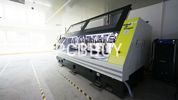
With the increase of signal transmission frequency, the surface thickness of the signal transmitted in the conductor becomes thinner and thinner, and when it is reached, the roughness of the traditional conductor surface no longer meets the requirements. Signal high-frequency makes signal transmission more and more concentrated in the wire surface, the faster the signal transmission frequency, the "surface layer" of the wire.
The thinner the transmitted signal. When the transmitted signal is transmitted only in the "roughness" dimension layer, then it is bound to produce serious signal "standing wave" and "reflection", so that the signal loss, the formation of serious distortion or complete distortion. Therefore, it is difficult to overcome this problem by continuing to use the traditional roughness surface. There are also anti-interference problems, and methods to improve surface roughness are also needed.
What Is the Bleaching Technique?
Overview of bleaching technology
The promotion and application of 4G and 5G communication technology has prompted the line width of printed circuit boards to enter the category of 10um. The influence of the roughness of electronic circuits manufactured by traditional etching method on signal integrity has become an important factor restricting the improvement of the electrical performance of terminal electronic products, especially in the high-frequency signal transmission system. The effect of blackening technology and brown technology on the treatment of copper surface is greater. It has been unable to meet the actual application needs, prompting the emergence of bleaching technology.
Bleaching technology belongs to a new generation of copper foil surface treatment technology. The main features are: a thin metallic tin layer is formed by copper surface replacement, and then a composite transition layer with stronger bonding force and resin substrate is formed on the surface of the treated copper foil, so as to achieve the dual purpose of improving the bonding force between the layers of multi-layer boards and the integrity of high-frequency signal transmission. Since the metal tin replaced by this technology on the copper surface is white, and the subsequent attachment of organosilane will not change the color of the line surface, it is called the bleaching technology. When metal Sn is replaced on the copper wire, considering that the binding force after electroless tin plating depends on the chemical bonding between the wire and the semi-cured sheet material, an organosilane layer should also be formed on the tin layer after tin plating to ensure high adhesion with the resin.
Different from blackening technology and brown technology, bleaching technology does not require serious physical or chemical etching on the surface of copper foil, but uses chemical tin plating and combined silane treatment to form a layer of non-etching bonding accelerator on its surface. Therefore, bleaching technology will not increase the surface roughness of copper foil during the treatment process. In this way, the goals of improving interlayer bonding force and effectively solving high-frequency signal transmission loss of high-frequency lines and fine lines are taken into account.
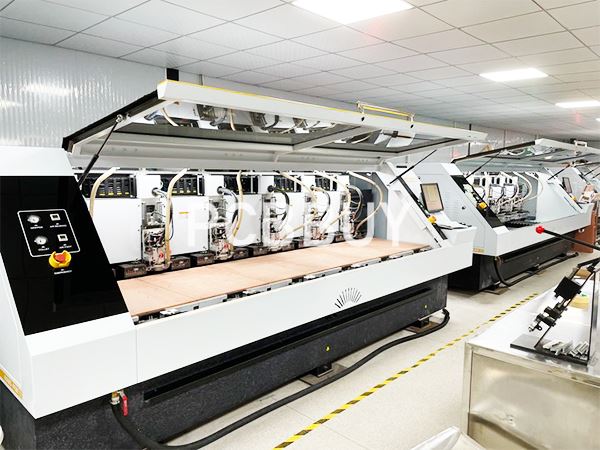
Introduction to whitening technology Applications
By testing the adhesion of the printed circuit board after bleaching, the adhesion of the bleaching process is better than that of the organic tissue of the etching process. It is found that in the frequency range of 3~5GHz, etching process results show greater signal loss than whitening process results, and the more the frequency is closer to high frequency, the more obvious the difference in signal loss.
By reducing the equipotential points of copper surface, whitening technology can promote the combination of copper surface and resin, on the one hand, reduce the surface roughness of the line, replace the etching process, and meet the requirements of fine lines. On the other hand, the output loss of high frequency signal is also reduced under the premise of ensuring the quality of the printed circuit board product.
Reference
He Wei, PCB Basic Electrical Information Science and Technology, China Machine Press,157-165
Industry Category


