How to Panelize PCB with 3 Effective Methods?
By:PCBBUY 09/24/2021 09:17

Manufacturing panels for printed circuit boards accomplish the same principle as those early polygraph duplicators by simultaneously creating multiple copies of a circuit board. To ensure that the benefits of these panels are maximized, PCB designers need to understand how best to lay out circuit board designs.
In this passage, check and read the content for more professional information to learn PCB panelization. If you are curious about this topic, welcome to read the content below.
What are the 2 main types of panel?
In general there are two different types of panels that can be used for the production of printed circuit boards. These differ with regard to the composition of the PCBs on the panel:
Homogenous composition (AAAA):
In homogenous assembly, the panel is composed of a multiplication of the same circuit board. This means that only one type of PCB is produced per panel. This is the most frequently used method in practice.
The popularity of this method is due to several important advantages: on the one hand, this method of assembly is independent of the manufacturing conditions and the product portfolio of the SMT manufactures. Secondly, the flexibility and effectiveness of the method is much higher than with any heterogenous composition of a panel.
Heterogenous composition (ABCD):
The panel is composed of a configurable mix of different printed circuit boards. This means that several types of PCBs can be produced simultaneously in a defined ratio.
An advantage of this composition is that stocks and buffers can be reduced with this method, since it is not necessary to provide a single panel for each type of PCB and a large number of PCBs do not have to be completed with each processing operation. On the other hand, it is difficult to control production differentiation and demand in a responsible way.
What are the 3 main methods of PCB panelization?
These factors limit the choices available to any one application. In fact, many assembly companies may use a combination of methods on any one project to ensure the structural integrity of the array while still mitigating issues during the breakout process.

The design of the board—namely how much component clearance is provided on the edges, whether sensitive SMT components are close to an edge, and whether or not connectors or other components hang over an edge—will limit the choices of panelization breakout methods from which to choose. Sometimes a combination of methods is appropriate to secure the PCB-array strength, while providing a viable breakout method.
To improve strength, increase the board count on the fabricator’s panel, and facilitate automated depaneling, arrays can be designed with solid tabs between boards in just about any orientation. The depaneling method for this kind of panel is either a depaneling router or a laser-cutting machine. The former creates vast amounts of dust, noise, and vibration, and requires firm holding fixtures. The latter is capital-intensive and limited to board thicknesses of about 1 mm. Still, these methods have their place in the high-volume market and aren’t subject to many of the restrictive guidelines to be outlined later.
There are three panelization techniques in use today, though only two are commonly practiced. They are:
1. V-Score Panelization
This common method of panelization separates individual PCBs with V-shaped grooves. These grooves remove approximately a third of the board’s thickness from the top and bottom of the board with an angled blade. A machine is commonly used to finish the breakout process, considering the remaining third of the board between the grooves is surprisingly strong, and hand-breaking can put stress on the PCB and surrounding components.

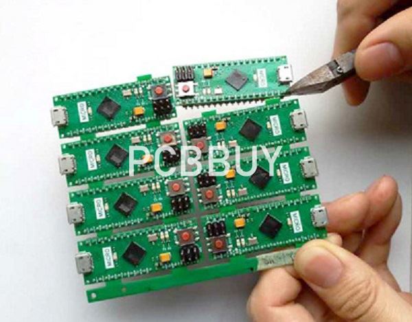
2. Tab Routing Panelization
PCB arrays that can’t feasibly use a V-groove method will instead use a tab routing method. With this method, PCBs are pre-cut from the array and held in place on the board with perforated tabs. Three to five holes are often used in these perforation patterns. This method is often beneficial for its ability to support designs with edge-hanging components. It can also be broken by hand instead of with tools.
3. Solid Tab Panelization
Arrays can be designed with solid tabs between each board, improving overall strength. However, the depaneling method for this type of panel requires either a depaneling router, a laser-cutting machine or a hook-shaped blade tool. The router can result in dust and vibration, while the laser-cutter is extremely expensive and ineffective on boards over 1mm thick. The hook-bladed option is less expensive but inefficient and prone to blade rotation. This method tends to be less common than the other two.
Industry Category


