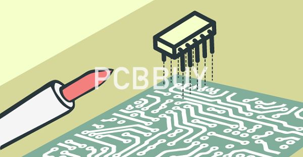
How to Place Components on PCB with whole 5 Essential Tips?
By:PCBBUY 10/15/2021 09:35

Placing components on a PCB isn’t a difficult task. First, you have to group the elements by function. Next, you need to keep the details away from the dissipating area. After that, make sure that you place the board-to-wire connectors near the edge. After that, get the orientation of the components standardized before finally making space for copper traces.
To learn more information about PCB components placement, you can check and read this passage for more professional knowledge. If you are interested in the PCB components placement, let’s check it!
1. What are the preparations for PCB components placement?
Before going into the specifics of test point and pad requirements, there are several general guidelines to keep in mind:
· Each node on your board should have at least one test probe point.
· It is not recommended to use component leads as test points.
· It is recommended to distribute your test points throughout your board.
· The spacing between test pads (center-to-center) should be maintained at 0.100”.
2. What is the importance of PCB components placement?
There’s a common saying that goes something like this – PCB design is 90% placement and 10% routing. This is entirely accurate. Taking the time to precisely place your components will make your life a whole lot easier when it comes time to route everything, while also giving your board its best electrical performance. But what happen if you just slap your components down without care?
· Hours Wasted. You’ll likely create a nightmare for yourself when you find out that some of your parts don’t even have enough space to be routed because you packed them too close together. The worst component placement jobs can lead to an entire board that needs to be started again from scratch.
· Busted Boards. Let’s say you do manage to place down some components and traces and ship your files off to your manufacturer. Next thing you know you might get a board back, that doesn’t work because your parts weren’t soldered correctly (more on this later).
· Ugly Aesthetics. Let’s face it, as engineers we love symmetry and precision, and there’s nothing more unsettling than seeing a board that wasn’t given some proper love and care during its component placement. It’s just plain lazy.

3. What are the common problems during of PCB components placement?
In general, the majority of component placement issues occur due to more complex routing and other issues. However, this is only one of the multiple issues requiring consideration:
· The component spacing: When placing components too close, it creates problems with automated pick-and-place, and it adversely affects testing (fixtures).
· May complicate depanelization: When components are too close to the board edge it may be hard to use routing to separate panels into individual boards.
· Makes rework harder: If rework is required, it is more difficult if components are not spaced well.
· A component’s location as well as orientation for wave soldering: If the component is discrete, both pins enter the solder simultaneously when the PCB goes through the wave. However, for larger components, they should not precede smaller components to avoid shadowing.
4. How to process effective PCB component placement?
You won’t have to deal with your mom’s nagging when you place components on PCB according to your whims and fancies. But be prepared to face a barrage of complaints from unhappy clients or technicians when problems crept up in the field.
Improper component placement can lead to a horde of issues that affect functionality, durability, manufacturability, and serviceability of the PCB. For example, placing analog and digital components without proper segregation is a perfect recipe for the analog signal to be compromised.

5. What are the basic guidelines of PCB component placement?
he majority of component placement problems that affect manufacturing are when components are placed too close to the edge of the board. This potentially can result in damage to the board from different sources, such as automated assembly equipment during a volume manufacturing run. Given below are some other placement considerations that you should keep in mind:
· Place your fixed parts first. These parts include anything that has to interface with the rest of the system that your board is going to be used in for example Connectors, switches, etc. Mechanical parts such as nuts and bolts will also need to be placed in fixed locations.
· Components placed too close together could cause problems for automated pick-and-place machines during assembly and for testing. Keep at least 50mil space between components and 100mil space from component to board edge.
· Try to place all components on the top side of the PCB. If not possible, only place small size and low thermal dissipation components (like SMD passive parts) can be on the bottom side.
· For groups of similar components place them in the same direction in evenly arranged rows or columns.
· Place decoupling capacitors as close as possible to VCC pin on active components.
Industry Category


