How to Prepare before PCB Prototyping?
By:PCBBUY 02/21/2024 16:31

Before you begin the PCB prototyping process, make sure that prototyping is right for your needs. While it is beneficial for many projects, it's not necessary for every type. If you decide to create a prototype, you'll need some basic information about your project to get started.
Electronic design businesses can benefit from faster turnaround time, as the manufacturing process for a PCB is far less labor-intensive than traditional circuit boards. Do you want to know the methods of PCB prototype? Please check and read the content below for more information in this passage.
How to Prepare before PCB Prototyping?
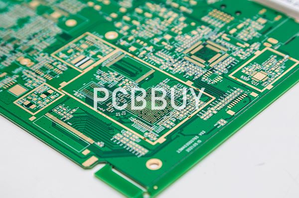
A prototype printed circuit board is an essential step in the design process of an electrical item. Printed circuit boards use conductive tracks to connect components. Printed circuit boards have lower manufacturing costs that traditional circuit boards. Because they are printed, there is no need for a complex wiring process.
Deciding If You Need a Prototype
Prototypes are ideal for when you want to test your design or perform a quality check of your board. You should use a prototype any time you use a new design for a new project. If you've already successfully produced an electronic product with that board, you may not need a prototype. If you make any design changes or create an entirely new PCB design or product, however, you should order a prototype.
Through our rapid prototyping service, we can build test boards with no more than eight layers and provide quality standard IPC1 boards using standard RF-4 material. For prototypes, we can fulfill orders of 5 to 100 pieces and offer a build time of four to five business days. Once you have approved your PCB prototype, you can order a full production of boards with more layers and different materials in greater quantities.

What Are the Common PCB Manufacturing Challenges?
Electronics and PCB manufacturing is presently facing several challenges together with opportunities. Along with the need to control costs, the PCB manufacturing services will have to focus on finding ways of capitalizing on current trends. This may include integrating technologies outside their primary areas of expertise, while meeting demands from customers for highly efficient manufacturing processes that are also eco-friendly. The biggest trends and challenges in the electronics manufacturing industries are likely to be:
Manufacturing is different from designing
The design of your PCB might look good on paper or a computer screen - but it can be an entirely different story when it comes to manufacturing it.
For example, there may not be sufficient tolerances between tracks on the board, which later on in the process could result in the circuit shorting out. Or perhaps the design includes a number of components positioned closely together, each with a different thermal mass. Achieving a quality solder joint on each of these components without heat damaging the rest of the circuit board requires expert process engineering skills.
If you are manufacturing a double-sided PCB, there are other factors to consider. Adopting this approach can allow you to fit more components into a limited space or to keep down costs. However, you will need to ensure that, where possible, your largest components are all placed on one side of the board and that this side is passed through the oven second. Otherwise, you risk these components falling off the board. You can use glue to hold down particularly difficult parts, but this requires additional manual work.
Insure the multilayer PCB stackup
Multilayer printed circuit boards are those boards that contain more than a single layer counts, hence the need for stack-up. Stack-up is the arrangement of insulating and copper layers to make a printed circuit board before the PCB layout design.
When it comes to the manufacture of multilayer printed circuit boards, challenges come in when it comes to pressing the insulating and copper layers together. A majority of multilayer printed circuit board manufacturers tend to encounter difficulties when it comes to pressing multilayer printed circuit board components together.

How to use PCB prototype board?
Perf Board
Perf boards are one of the available types of prototype boards. This category is also known as the “Pad per hole” design, where each hole has its own conductor pad made from copper with it. With this setup, you can test connections by running solder between individual pads. Additionally, you can also run wires between pads on a perfboard as well.
Stripboard
Like the other common type of prototype PCB, stripboards also have the individual hole set up. Instead of each perforation having a single conductor pad, strips of copper run parallel under the length of the board to connect the holes—hence the name. These strips substitute as wires, and you can also break connections as well.
Planning
Even if you know how to use a PCB prototype board, you don’t want to drive straight into building one. While protoboards are way less costly than a printed circuit board, they still have more permanent configurations. Before you get started putting components into place, you should spend some time on the planning stage to give yourself the best results.
A straightforward way to get started is to use a board-planning application on your computer. Software like this gives you a choice to visualize circuits before putting any components down. Be aware that some programs are suitable for working with both perf and stripboard, while others only work well with one type, so plan your protoboard purchases accordingly.
Industry Category


