How to Prepare for PCB Design Interview Questions with 5 Useful Tips?
By:PCBBUY 12/01/2021 09:57

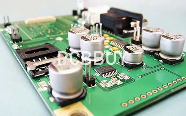
A PCB designer is responsible for taking a 2D schematic and creating the 3D CAD files used to manufacture the PCB. The first step is to create the component footprints, which show the size, shape, and orientation of each component. Second, the PCB designer creates a board outline with the dimensions and shape of the board as well as any keep out areas. Then the components with critical placement requirements are locked down, such as connectors that have to match up with another board.
If you're interested in becoming a PCB designer, one of the first things to consider is how much education you need. We've determined that 29.2% of PCB designers have a bachelor's degree. In this passage you will get to know the common questions about the PCB design interview. Come and check the content below for more.
What are the considerations of PCB design interview?
There are, however, other types of interviews as well. You may be interviewing someone to work for you or you may be vetting a service provider such as a PCB contract manufacturer. Interestingly enough, many of the questions in these interviews will be the same. Before we look at those questions, let’s go through some basic interview tactics first:
· Be prepared before you start. This isn’t just a matter of having a list of questions, it is also knowing what it is that you are looking for and what you expect the results to be.
· Make the person you are interviewing with feel comfortable. An interview shouldn’t be a matter of ambushing someone to get the right answers. Instead, it should be an honest exchange of information to evaluate whether or not there will be a good fit.
· If you are being interviewed, you should be prepared with examples of your work as well as questions about the company culture and workflow.
· If you are interviewing others, set a realistic schedule and agenda for your meeting. You want to spend enough time so as to cover the topic thoroughly, while at the same time not repeating the same questions.
· Finally, don’t be afraid to blow your own horn when you are being interviewed. If what you’ve done is important, make sure that a potential employer knows about it. After all, no one else in the room is going to know about it. Just be careful that you don’t blow that horn too loudly or too long.
What are the common questions of PCB design interview?
What are the inputs you need to design a PCB?
A: We need schematic,bom and netlist(some pcb engineer generates netlist) from Hardware side and Board mechanicals from client i.e, board outline,mounting holes etc.
and another important thing that we need is PCB stackup it is based on complexity of the board for example if we are using fpga first we should know number of signal layers need for fpga signal breakout.

How to create footprint?
A: Footprint flow:
· Padstack creation
· Pin placement
· Assembly outline
· Silkscreen outline
· Place bound top (we can mention height of the here)
· DFA bound top
· No probe top
· Silk and assembly reference designator
How to avoid high-frequency interference?
A: The leading principle to overcome high-frequency interference is to reduce crosstalk as much as possible, which can be achieved by enlarging the distance between high-speed signals and analog signals or equipping ground guard or shunt traces beside analog signals. In addition, the noise interference caused by digital ground on analog ground should be carefully considered.
How to arrange traces carrying differential signals?
A: Two points should be focused in terms of traces carrying differential signals design. On one hand, the length of two lines should be the same; on the other hand, the spacing between two lines should maintain parallel.
How to arrange traces carrying differential signals when there’s only one clock signal line at output terminal?
A: The premise of traces carrying differential signals arrangement is that both signal sources and receiving end should be differential signals. Therefore, differential routing can never work on clock signals containing only one output end.

Can matched resistance be added between differential pairs at receiving end?
A: Matched resistance is usually added between differential pairs at receiving end and its value is equal to that of differential impedance. As a result, signal quality will be better.
Why should differential pair traces be close to each other and parallel?
A: Differential pair traces should be properly close and parallel. The distance between differential pair traces is determined by differential impedance that is a key reference parameter in terms of differential pair design.
In the process of high-speed PCB design, which measures should be taken in consideration of EMC/EMI?
A: Generally speaking, EMI/EMC design should be considered from both radiated and conducted aspects. The former belongs to the portion whose frequency is higher (more than 30MHz) while the latter to the portion whose frequency is lower (less than 30MHz). Therefore, both high-frequency portion and low-frequency portion should be noticed. A good EMI/EMC design should start from components’ placement, PCB stack up, routing, component selection etc. Once those aspects leave unconsidered, cost will possibly rise. For example, clock generator should not be close to exterior connector as much as possible. Additionally, connecting points should be properly selected between PCB and chassis.
What is routing topology?
A: Routing topology, also called routing order, refers to the order of routing in terms of network with multiple terminators.
How routing topology should be adjusted to increase signal integrity?
A: This type of network signals is so complex that topology is different based on different directions, different levels, and different kinds of signals. Therefore, it’s difficult to judge which type of signals is beneficial to signal quality.

How to successful prepare for PCB design interview?
Although this question is more targeted towards vetting a new service provider, you should also expect it in job interviews. You need to know what a vendor or a potential employee can do, so prepare questions that will cover the needs that you want to be highlighted. For instance, can your manufacturer handle a tight schedule for a prototype build, or does your engineering prospect have experience with rigid-flex designs? And when you are interviewed count on being asked what exactly it is that you are capable of doing. Be prepared to give honest and direct answers as no one wants to find out after you’ve been hired that you weren’t completely up-front with them.
Industry Category


