How to Prevent PCB Warpage with 7 Basic Important Tips?
By:PCBBUY 07/30/2024 17:26
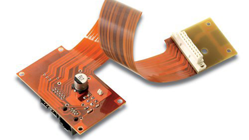
PCB warpage is a critical issue in the electronics manufacturing industry that can significantly affect the performance and reliability of electronic assemblies. Warpage refers to the deformation of the PCB substrate, leading to an uneven surface that can cause alignment issues, poor solder joints, and mechanical stress on components. This article provides an in-depth examination of PCB warpage, its causes, and seven essential tips to prevent it. These tips are rooted in industry knowledge and supported by technical data, ensuring a comprehensive understanding for designers and manufacturers alike.
Do you know how to prevent the PCB warpage? If you are curious about the methods to prevent the PCB warpage, please check and read the content below for more information.
What is PCB Warpage?
PCB warpage occurs when a printed circuit board deviates from its intended flatness, resulting in a bend or twist. This deformation can compromise the board's mechanical integrity and electrical performance, leading to various issues such as:
Component misalignment
Poor solder joint quality
Increased mechanical stress on components and interconnections
What Are the Causes of PCB Warpage?
Warpage can result from various factors, including:
Material properties: Different materials have varying coefficients of thermal expansion (CTE), which can cause warpage when subjected to temperature changes.
Uneven copper distribution: Asymmetric copper layers can lead to uneven thermal expansion and contraction, causing warpage.
Manufacturing processes: Improper handling during the lamination, soldering, or cooling processes can introduce stresses that lead to warpage.
Seven Essential Tips to Prevent PCB Warpage
Tip 1: Choose the Right Materials
Understanding Material Properties
The choice of materials significantly influences PCB warpage. Key material properties include:
Coefficient of Thermal Expansion (CTE): A measure of how much a material expands or contracts with temperature changes.
Glass Transition Temperature (Tg): The temperature at which a material transitions from a rigid state to a more plastic state.
|
Material |
CTE (ppm/°C) |
Tg (°C) |
|
FR-4 |
14-18 |
130-180 |
|
Polyimide |
3-5 |
200-260 |
|
200-260 |
6-8 |
150-200 |
Material Selection Guidelines
Low CTE Materials: Opt for materials with lower CTE to minimize thermal expansion differences.
High Tg Materials: Use materials with high Tg to ensure dimensional stability under high temperatures.
Tip 2: Optimize Layer Stack-Up and Copper Distribution
Balanced Layer Stack-Up
A well-balanced layer stack-up is crucial for minimizing warpage. It involves:
Symmetrical Layer Arrangement: Ensuring that the layers are symmetrical around the center of the board to balance thermal stresses.
Uniform Copper Distribution: Equalizing copper distribution across the layers to prevent localized stresses.
|
Layer Number |
Layer Type |
Copper Thickness (oz) |
|
1 |
Signal |
1 |
|
2 |
Ground |
1 |
|
3 |
Power |
1 |
|
4 |
Signal |
1 |
Techniques for Copper Balancing
Use of Dummy Copper: Adding non-functional copper areas to balance the copper distribution without affecting electrical performance.
Design Considerations: Plan the layout to avoid large copper-free areas, which can lead to differential expansion.
Tip 3: Control the Lamination Process
Lamination Temperature and Pressure
The lamination process involves pressing and heating the PCB layers together. Key factors include:
Temperature Control: Ensure consistent lamination temperature to avoid thermal gradients.
-Pressure Application: Apply uniform pressure to prevent layer shifting or air entrapment.
|
Parameter |
Recommended Value |
|
Temperature |
170-200°C |
|
Pressure |
250-300 PSI |
|
Time |
250-300 PSI |
Quality Control Measures
Pre-Lamination Inspection: Check materials and layers for any defects or inconsistencies.
Post-Lamination Inspection: Inspect for uniformity, voids, or delamination.
Tip 4: Implement Proper Cooling Techniques
Controlled Cooling Rates
After lamination and soldering processes, controlled cooling is essential:
Gradual Cooling: Prevents thermal shock and reduces internal stresses.
Use of Cooling Fixtures: Ensures that the PCB cools down evenly, maintaining flatness.
|
Cooling Method |
Cooling Rate |
Application |
|
Natural Air Cooling |
Slow |
General applications |
|
Forced Air Cooling |
Moderate |
High-volume production |
|
Fixture-Assisted |
Controlled |
High-precision boards |
Avoiding Rapid Temperature Changes
Rapid cooling can induce warpage due to differential contraction rates between materials. Use gradual cooling techniques to minimize these effects.
Tip 5: Proper Handling and Storage
Handling Practices
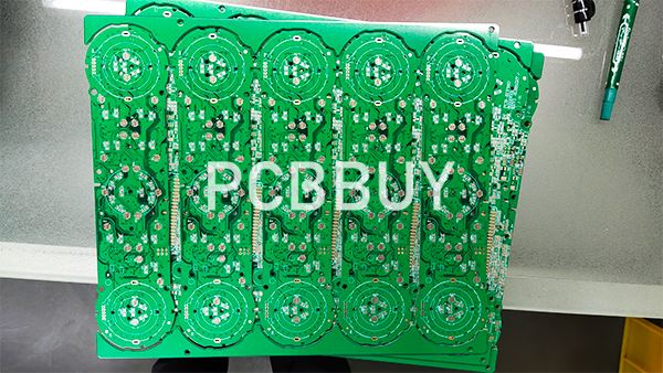
Minimize Flexing: Avoid bending or flexing the PCB product during handling to prevent mechanical stress.
Use Support Tools: Use fixtures or trays to support the PCB during transportation and handling.
Storage Conditions
Controlled Environment: Store PCBs in a temperature and humidity-controlled environment to prevent moisture absorption.
Flat Storage: Store PCBs on flat surfaces to avoid bending or warping over time.
|
Condition |
Recommended Range |
|
Temperature |
20-25°C |
|
Humidity |
30-50% |
|
Storage Orientation |
Flat, no bending allowed |
Tip 6: Design for Manufacturability (DFM)
DFM Guidelines
Component Placement: Avoid placing heavy components in areas prone to warpage. Distribute weight evenly across the board.
Thermal Reliefs: Use thermal relief pads for component leads to reduce thermal stress during soldering.
|
Design Aspect |
Best Practice |
|
Component Placement |
Even distribution |
|
Thermal Reliefs |
Use for large pads |
|
Trace Design |
Avoid large copper areas |
Prototyping and Testing
Prototyping: Build prototypes to test for warpage and make necessary design adjustments.
Thermal Cycling Tests: Subject PCBs to thermal cycling to evaluate their warpage resistance.
Tip 7: Use Advanced Manufacturing Techniques
Automated Optical Inspection (AOI)
Early Detection: Use AOI to detect warpage and other defects early in the manufacturing process.
Corrective Actions: Implement corrective measures based on AOI findings.
|
Inspection Method |
Advantages |
|
AOI |
Non-destructive, high accuracy |
|
X-ray Inspection |
Internal defect detection |
Innovative Manufacturing Solutions
Flexible PCB Designs: Consider using flexible or rigid-flex designs to reduce stress points and accommodate slight warping.
3D Printing: Explore the use of 3D printing for creating complex PCB designs with reduced warpage risk.
Conclusion
Preventing PCB warpage is essential for ensuring the reliability and longevity of electronic assemblies. By following these seven important tips, designers and manufacturers can minimize the risk of warpage, resulting in better product performance and reduced failure rates. These tips encompass material selection, design optimization, manufacturing process control, and advanced inspection techniques, providing a comprehensive approach to warpage prevention.
References
1. IPC-6012, "Qualification and Performance Specification for Rigid Printed Boards," IPC, 2020.
2. IPC-2221, "Generic Standard on Printed Board Design," IPC, 2021.
3. A. DiGiovanni, "Printed Circuit Board Materials Handbook," McGraw-Hill, 2009.
4. J. H. Lau, "High-Density PCB Design and Fabrication," McGraw-Hill, 2003.
5. K. Gilleo, "Area Array Packaging Handbook: Manufacturing and Assembly," McGraw-Hill, 2002.
Industry Category


