How to Prevent Solder Bridging with 5 PCB Manufacturing Process Steps?
By:PCBBUY 09/11/2021 10:08

The same precision is necessary when assembling components on a PCB. Not only must the components be placed accurately on top of the pads, but the soldering process must be equally flawless, otherwise, you’ll stumble into all sorts of soldering issues, including solder bridging.
In this passage, we will provide you the methods of preventing the solder bridging and the main steps of the PCB manufacturing process. If you are interested in this topic, please check and read the content we prepare for more information.
Depending on the manufacturer, the PCB manufacturing process may differ slightly, especially in terms of component mounting techniques, testing methods, and so on. They are manufactured in bulk quantities using various automated machines for drilling, plating, punching, and so on.
What are the reasons of solder bridging?
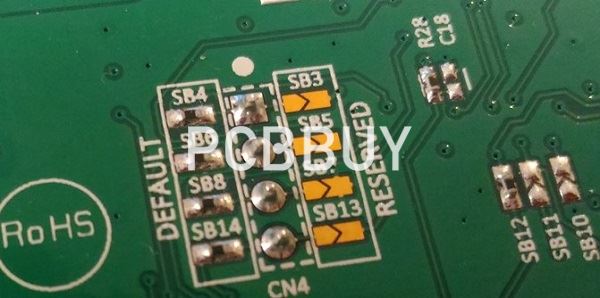
The issue can be aggravated if the solder paste mask is absent or only covers a narrow area between the pads. This enables the solder paste to rest on the substrate, which causes solder bridges to easily form.
Sometimes, solder bridging is caused by stencil thickness, which affects the volume of solder paste applied onto the pad. A thicker stencil will lead to more solder paste on the pads, which may cause the paste to overflow from one pad to another.
Correctly built footprints
Solder bridging can be a result of problems with the component footprints used in PCB design, as well as how those parts are placed on the board. Here are some design recommendations that can help: Be careful to use industry specified pad sizes on your PCB footprints to ensure that a good solder joint can be formed. A surface mount pad must have a correctly sized solder paste shape defined for it to create the right sized aperture in the solder stencil.
Make sure that each pad in a PCB footprint has the correct sized solder mask definition built into it for full solder mask protection. Footprint pads should have enough spacing between them for the even application of solder mask between the pads.
Solder Mask Defined Pads
In instances (BGAs or LGAs) where you need a solder mask dam between two SMT pads, but lack the necessary room to maintain mask relief and a barrier, try using a zero solder mask expansion setting for your pads. These provide a solder mask relief that is the same size as the copper pad it is protecting.
If this is the case, you should note this in your fabrication files, thus informing your CM to leave the solder mask defined pad as is, i.e., no standard mask clearances.
Fiducial Markers
Fiducial markers are specific design markers or indicators that you utilize in the PCB design process. These alignment markers ensure that components place accurately in terms of orientation and alignment with pads. When coupled with adequate design clearances, these markers minimize the likelihood of solder bridging occurrences.

What are the 5 key steps of PCB manufacturing?
1. Etch Your PCBs
PCBs are made by bonding a copper layer over the entire substrate. Sometimes, both sides of the substrate are covered using copper layers. The PCB etching process, also called a controlled horizontal process, is carried out to remove excess copper from the PCB panel using a temporary mask. After the etching process, the circuit board is left with the desired copper traces.
2. Stripping Process of PCBs
Even after the etching process, some amount of copper remains on the circuit board, which gets covered by tin/lead or electroplated tin. Nitric acid removes tin effectively while maintaining the copper circuit cracks below the tin metal. As a result, you will get a clear distinct copper outline on the circuit board, and the circuit board is ready to be passed on to the next process – Solder Resist.
3. Solder Resist
This is one important process in the PCN designing process, which covers unsoldered areas on the circuit boards using solder resist material. As a result, it prevents the solder from forming traces, which can create shortcuts to adjacent component leads.
4. PCB Testing
After the PCB is manufactured, testing becomes crucial to check the functioning and features. In this method, the PCB manufacturer determines whether the circuit board is working as expected. Today, PCBs are tested using several advanced testing equipment. ATG test machine is mainly used for testing high volume PCB route, which include flying probes and fixtureless testers.
5. PCB Assembling
This is the last step of PCB manufacturing which mainly includes the positioning of various electronic components on to their respective holes. This can be carried out by either through-hole technology or surface mount technology. One common aspect of both the techniques is that the leads of the component are fixed electrically as well as mechanically to the circuit board using a molten metal solder.
Industry Category


