How to Print Silkscreen on PCB through 5 Effective Methods in Manufacturing Process?
By:PCBBUY 11/10/2021 09:40

As discussed earlier, using a silkscreen PCB layout is an important aspect of board design and not including it can cause serious problems for PCB assembly and testing. The silkscreen is also used for labeling, which may include manufacturer information, testing certifications, model or serial numbers. In order to be effective and useful, the silkscreen must have clearly readable text, provide sufficient image resolution and, most importantly, be accurate.
Are you curious about the methods of silkscreen PCB? If you are going to learn more about how to process silkscreen PCB, please check and read the content below for more professional knowledge.
1. What is the basic knowledge of silkscreen on PCB?
With technological advancement, the text and beautification images can also be part of silkscreen artwork design. However, the pitfall is that you may overlook the fundamental purpose of the design and may make the information unreadable easily.
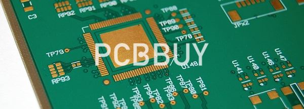
During the manufacturing process of PCB, silkscreen is marking ink used to identify components during later assembly and troubleshooting processes. This can be placed on one or two sides (in yellow or white), depending on the board design and application.
The silkscreen layer is the top layer of the PCB and serves as a reference indicator for placing components on the PCB. Screen printing is used to specify useful information on the PCB board, which can help users during the assembly. It is used to mark component values, part numbers, test points, polarity, etc.
2. What are the specifications of silkscreen on PCB?
A silkscreen may not have any role in the functioning of a PCB; however, it is valued for the information that it delivers. For instance, it will help anyone to:
· Understand the warning symbols
· Polarity of parts
· Identify the test points
· Locate the parts through reference designators
· Identify the numbers that are unique to the printed circuit board.
· Identify manufacturer marks, version numbers, and so on
3. What is the importance of silkscreen on PCB?
Though the Silkscreen has nothing to do with the functionality of the Printed Circuit Board, the PCB Silkscreen provides information on

· Warning Symbols – The warning symbols indicate the parameters on the high voltage points that you need to avoid or handle.
· Polarity Indicators – It helps you to trace the polarized component’s orientation.
· Locating the parts via reference designators
· It helps in identifying the test points and unique numbers for each board.
· Reference indicators – It helps in identifying the component types via BOM. The Pin 1 indicator helps you to connect the pins to the suitable pads in the footprint. The leading pattern of the component outline would show the placement of a component. The polarity indicators provide you with the polarized component’s orientation
· Pin 1 indicator – It indicates the connection of pins on the correct pads of the footprints.
· Component Online – It enables you to place the components on PCB through indications.
The Component Online wouldn’t be essential for simpler components having a smaller number of pads. However, you would need them for general placement. But you can’t miss out on indicators, Pin 1, Polarity indicators.
4. What are the methods of silkscreen on PCB?
In the past few years, the primary method of silkscreen referred to using a stencil to directly apply ink to the board surface. Nowadays, there are the two most common silkscreen PCB printing techniques, such as liquid photo imaging (LPI) and direct legend printing (DLP).
Liquid photo imaging (LPI):
This method is used when the line widths are greater than 4 mil. Liquid Photo Imaging is quite similar to the process used for the application of solder mask. In this a liquid photo-imageable epoxy is coated on to the laminate and then exposed with UV light. After this the board is developed and cured. It is much more accurate than manual screening
Direct legend printing (DLP):
DLP is the most accurate of all these processes but is more expensive. In this process an inkjet projector is used with acrylic ink that is applied onto the raw PCB directly from the CAD data. The ink is cured with UV light as it is printed. It should be noted though that the acrylic ink does not cure on boards with silver finishes.

5. How to apply silkscreen on PCB?
Manual Screen-printing
Manual screen-printing is done when the line widths are greater than 7 mil (0.007”) and the registration tolerance is 5 mil. For this method you require a stencil of the text and traces made of nylon. The ink is pushed through the stencil onto the laminate. Next the board is baked in a curing oven for the ink to cure.
Liquid Photo Imaging (LPI)
This method is used when the line widths are greater than 4 mil. Liquid Photo Imaging is quite like the process used for the application of solder mask. In this a liquid photo-imageable epoxy is coated on to the laminate and then exposed with UV light. After this the board is developed and cured. It is much more accurate than manual screening.
Direct Legend Printing (DLP)
DLP is the most accurate of all these processes but is more expensive. In this process an inkjet projector is used with acrylic ink that is applied onto the raw PCB directly from the CAD data. The ink is cured with UV light as it is printed. It should be noted though that the acrylic ink does not cure on boards with silver finishes.
Industry Category


