By:PCBBUY
03/10/2022 10:03
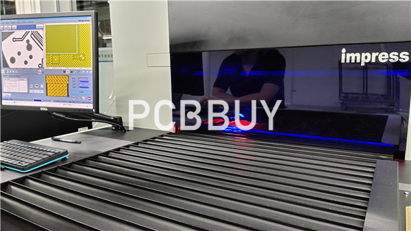
AOI checks circuit boards by using multiple light sources and one or more cameras (either still or video). The lights shine on the board from different angles, and the cameras take pictures or videos. These images are put together to show the whole board. Then, the system compares what it sees with the design plans or a sample of a good board to find any problems.
PCB Instant Quote
In this passage,this part explains the professional basics of Automated Optical Inspection for PCBs during production. If you need more details about AOI for PCBs, keep reading the following content.

What is the Automated Optical Inspection on PCB?
Automated Optical Inspection (AOI) on PCB (Printed Circuit Board) is a crucial quality control technology used in PCB manufacturing, which inspect PCBs for defects or errors, replacing or supplementing manual inspection.
Hardware Setup:
Light Sources: Multiple lights (e.g., LED, halogen) illuminate the PCB from various angles to highlight different features and potential defects.
Cameras: One or more high-resolution still or video cameras capture images of the PCB surface. These cameras may use different technologies (e.g., 2D, 3D) to inspect both the top and bottom layers, as well as component profiles.
Image Acquisition:
The lights and cameras work together to capture detailed images of the PCB, including soldered components, traces, vias, and solder joints. Images from different angles are combined to form a comprehensive view of the board.
Image Processing and Analysis:
Missing components or incorrect placement.
Solder defects (e.g., bridges, insufficient solder, cold joints).
Damaged traces or misaligned features.
Component polarity errors (e.g., reversed resistors or capacitors).
The system compares the captured images against a “golden standard” (a reference model based on design specifications or a previously approved, defect-free PCB). It uses algorithms to identify deviations, such as:
Defect Detection and Reporting:
If discrepancies are found, the system flags the defects, often indicating their location and severity. This information helps manufacturers correct issues promptly, reducing rework and improving yield.
Enhanced Quality Control: Detects tiny defects that are hard to spot manually, ensuring PCBs meet design standards.
Faster Inspection: Automates the process, reducing production time compared to manual inspection.
Consistency: Provides uniform inspection results, eliminating human error or subjectivity.
Data Collection: Generates detailed reports that help identify trends (e.g., recurring defects) to optimize manufacturing processes.
Cost Savings: Prevents costly errors in later production stages (e.g., after assembly) by catching issues early.
AOI is typically used at various stages of PCB production, including:
After solder paste printing: To check paste volume and placement accuracy.
After component placement: To verify component positioning and polarity.
After reflow soldering: To inspect solder joint quality and component integrity.
2D AOI: Uses 2D images to inspect planar features (e.g., component presence, solder paste geometry).
3D AOI: Incorporates depth-sensing technology (e.g., laser triangulation, structured light) to inspect 3D aspects like component height and solder joint shape.
Complexity of Modern PCBs: Denser layouts and smaller components (e.g., micro-BGA) require higher-resolution cameras and advanced algorithms.
Calibration and Setup: Proper configuration of light sources, camera angles, and inspection parameters is critical to avoid false positives (incorrect defect flags) or negatives (missed defects).
Integration with Production Lines: AOI systems must integrate seamlessly with other manufacturing equipment (e.g., pick-and-place machines) for efficient workflow.
In summary, AOI on PCB is a vital automated technology that ensures the reliability and quality of PCBs by visually inspecting them for defects, enabling manufacturers to produce higher-quality products with fewer errors.
Low cost: AOI test can improve the pass rate of PCB so that reduce the PCB cost.
