How to Process PCB Panel for Manufacturing?
By:PCBBUY 03/07/2024 16:11

As a result of mass production, PCB panelization enables you to save money and time. The cost of building many boards in large panels of multiple boards is more cost-effective than building them singularly. The core advantage of penalizing several projects is to save money. There are shipping and tooling costs for different projects, and if you have several un-panelized printed boards, it means that you will pay these fees multiple times.
In this passage, we are going to tell you all about the methods of PCB panel. If you are looking for more about PCB panel, please check and read the content below for more professional knowledge.
What is the structure of PCB panel?
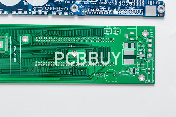
A panel consists of one or more printed circuit boards, which are either completely connected or connected to each other via residual bridges.
A distinction is made between scoring or notched panels and milling panels with retaining bridges. Additional holes in the residual bridges facilitate the singulation of the boards later on. A combination of scoring and milling is useful (if feasible) to reduce the milling costs to a minimum.
The position and number of bridges must be carefully determined in relation to the panel or PCB size, component position and PCB thickness in order to ensure both sufficient stability and the simulation of the PCBs from the panel with as little mechanical stress as possible for the solder joint and the component.
What is the necessary for PCB panel?
Save money and time
As a result of mass production, PCB panelization enables you to save money and time. The cost of building many boards in large panels of multiple boards is more cost-effective than building them singularly. The core advantage of penalizing several projects is to save money. There are shipping and tooling costs for different projects, and if you have several un-panelized printed boards, it means that you will pay these fees multiple times.

However, if you have multiple projects in large panels on a single printed board, you will pay the fees just once. Since your boards are in large groups and are together, you can ship them simultaneously, which helps save the shipping costs that would occur with separate shipments. By getting all your boards in a single, large panel, it means that the rapid-fire pick and place machine will get all the components of the printed boards at a go. It helps save setup time.
Improves work efficiency
As a way of improving the productivity of the PCB manufacturing process, it is common practice to mount several copies of smaller printed circuit boards in a manufacturing panel. It is an effective method of fabricating and assembling the boards instead of building them one by one. The panel must contain the same materials and layer stack-up configuration as the printed board.
It is also essential to choose the size of the panel, whether small or large, that best fits your printed circuit board's needs and the various manufacturing and assembly processes. The more boards you can fit into a PCB panel, the more efficient the manufacturing process will become. It will also reduce the number of panel space that will go to waste.
During panelization, PCB panel designers must use all the arrangement options when placing the PCB designs to optimize the panel space and improve manufacturing efficiency.
How to Process PCB Panel for Manufacturing?
PCB Panelization gives great benefits to PCB producers. It saves cost as well as assembly time, human effort, material cost and hence time-to-market of product.

A PCB for large scale production purposes i.e., for massive production of single PCB in form of PCB array is connected together physically as in Figure 1 and Figure 2. It makes it easier to move PCBs array across the assembly line much like a electronic component tray. The individual boards are easily separable after assembling for QC-inspection or to fit into the product enclosure. For production of tens of thousands of PCBs, component placement for PCB Panelization also does matter. Especially connectors and components hanging off the boundaries of PCB can create difficulty in PCB assembling process.
PCB Shape and size
Some PCB assembly contractors require minimum size of PCB to fit in a conveyor. A smaller size PCB which cannot fit physically within conveyor is needed to add small catch-in-hold area for processing. This extra PCB area is removed after PCB assembling. The situation is more complex in case of odd shaped PCBs. The rectangular PCB shape does fit easily in a panel however curved and odd-shaped PCBs need also some extra PCB area for handing by SMT conveyor. This situation can complicate PCB Panelization or assembly. Rectangular PCBs can be placed ideally both in vertical and horizontal axis. The CAD Software tools alongwith guidance of manufacturer and assembler can lead to early time measures. By involving manufacturer, assembly and PCB design engineer maximum benefits can be reaped.
Panel Space
Typically PCB manufacturers run standard panels sizes like 24 x 18 inches. They need 0.5 inches clearance from components on the perimeter of panel. So 23 x 17 inches Panel size is actually available panel space for manufacturing. They need small gaps i.e., 0.1 inches for routing board arrays which is another unusable panel space. The PCB developer may get help to use panel space effectively by using calculation Tools available by manufacturers or online.
Industry Category


