How to Process PCB Panel for Manufacturing?
By:PCBBUY 09/27/2024 15:23
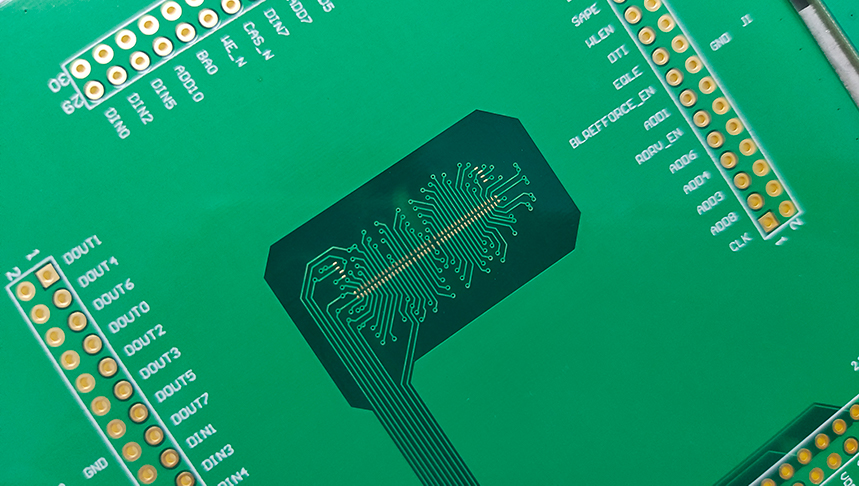
The processing of Printed Circuit Board (PCB) panels is a critical step in electronic manufacturing. This article will detail the procedures involved in PCB panel processing, from initial design to final fabrication, while covering the underlying principles, necessary chemical processes, and data-driven comparisons.
1. Understanding PCB Panels
1.1 What is a PCB Panel?
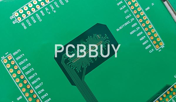
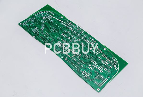
A PCB panel consists of multiple individual PCBs laid out on a single substrate, designed to optimize the manufacturing process. These panels are essential for mass production, reducing waste and improving efficiency.
1.2 Types of PCB Panels
PCBs can be categorized based on their construction:
Single-sided PCBs: Contain circuits on one side.
Double-sided PCBs: Have circuits on both sides.
Multilayer PCBs: Include multiple layers, increasing complexity and functionality.
Table 1: Comparison of PCB Types
|
PCB Type |
Layers |
Applications |
Cost |
|
Single-sided |
1 |
Simple electronics |
Low |
|
Double-sided |
2 |
Moderate complexity devices |
Moderate |
|
Multilayer |
3 |
High-performance applications |
High |
2. Design and Layout
2.1 CAD Design
The design phase begins with Computer-Aided Design (CAD) software to create PCB layouts. Important considerations include:
Component Placement: Optimizing space for performance and manufacturability.
Trace Width and Spacing: Ensuring electrical reliability and minimizing interference.
2.2 Design Rules
Design rules are essential for ensuring manufacturability. Common guidelines include:
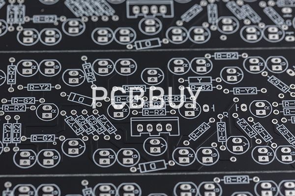
- Minimum trace width: Typically, 0.2 mm for standard PCBs.
- Minimum spacing: At least 0.2 mm to prevent short circuits.
3. PCB Fabrication Process
3.1 Material Selection
Selecting the right materials is crucial for performance and reliability. Common materials include:
Substrate: Typically FR-4, a composite of glass fiber and epoxy resin.
Copper Foil: Used for conductive pathways, typically 1 oz/ft² for standard applications.
3.2 Manufacturing Steps
The PCB fabrication process consists of several key steps:
3.2.1 Printing the Design
The first step involves printing the PCB design onto the substrate using photolithography. The process includes:
1. Coating with Photoresist: A light-sensitive material that allows selective removal.
2. Exposure to UV Light: Transferring the design onto the photoresist layer.
3.2.2 Developing the Photoresist
After exposure, the board undergoes development to remove unexposed areas of the photoresist, revealing the copper layer beneath.
3.2.3 Etching
The exposed copper is then removed through chemical etching, using a solution of ferric chloride (FeCl₃) or ammonium persulfate (NH4)2S2O8:
Cu + FeCl3 →CuCl2 + FeCl2
3.3 Plating and Coating
After etching, the PCB is plated to enhance conductivity. Key processes include:
Electroless Plating: Depositing copper in the holes.
Surface Finishing: Applying finishes such as HASL or ENIG for solderability.

4. Assembly of PCB Panels
4.1 Component Placement
Components are placed on the PCB using automated pick-and-place machines. Accurate placement is crucial for soldering and functionality.
4.2 Soldering Techniques
Common soldering methods include:
Wave Soldering: Suitable for through-hole components, where the PCB is passed over a wave of molten solder.
Reflow Soldering: Used for surface mount devices (SMD), where solder paste is applied and heated.
Table 2: Comparison of Soldering Methods
|
Soldering Method |
Efficiency |
Suitable Components |
Cost |
|
Wave Soldering |
High |
Through-hole components |
Moderate |
|
Reflow Soldering |
Very High |
Surface mount devices |
High |
5. Testing and Quality Assurance
5.1 Functional Testing
Functional testing ensures that each PCB operates according to specifications. Methods include:
In-circuit Testing (ICT): Checks for shorts and opens in the circuit.
Automated Optical Inspection (AOI): Verifies component placement and solder quality.
5.2 Reliability Testing
Reliability testing evaluates PCB performance under stress, including:
Thermal Cycling: Subjecting PCBs to temperature variations to identify potential failures.
Mechanical Shock Testing**: Assessing the durability of solder joints.
Conclusion
Processing PCB panels involves intricate design, precise fabrication, and thorough testing to ensure high-quality electronic products. Understanding each step, from material selection to assembly and testing, is vital for manufacturers to produce reliable PCBs.
References
1. Friedman, A. (2019). "PCB Design and Manufacturing: A Comprehensive Guide." Journal of Electronic Materials.
2. Hwang, J. (2020). "Advancements in PCB Technology: Challenges and Solutions." International Journal of Electronics.
3. Katz, R. (2021). "The Science Behind PCB Fabrication." Journal of Materials Science.
4. Liu, Y. (2022). "Reliability Testing of PCBs: Methods and Standards." IEEE Transactions on Components, Packaging and Manufacturing Technology.
5. Sullivan, J. (2023). "Soldering Techniques in PCB Assembly." Soldering & Surface Mount Technology.
Industry Category


