How to Process PCB Troubleshooting?
By:PCBBUY 03/31/2025 14:36
Introduction
Printed Circuit Boards (PCBs) are the backbone of modern electronics, found in everything from smartphones to industrial machinery. However, like any complex system, PCBs can develop faults due to design flaws, manufacturing defects, or environmental factors. Effective troubleshooting is essential to ensure reliability and performance.
This guide provides a detailed, step-by-step approach to PCB troubleshooting, covering fundamental principles, common failure modes, diagnostic techniques, and repair strategies. We also include data-driven insights and comparison tables to enhance understanding.
1. Understanding PCB Faults: Common Causes and Symptoms
1.1 Common PCB Failure Modes
PCBs can fail due to multiple reasons, broadly categorized as:
|
FailureCategory |
Examples |
Symptoms |
|
Manufacturing Defects |
Poor solder joints, misaligned components |
Intermittent connections, overheating |
|
Design Flaws |
Incorrect trace width, insufficient grounding |
Signal integrity issues, EMI interference |
|
Environmental Stress |
Moisture, thermal cycling, vibration |
Corrosion, cracked traces, component failure |
|
Electrical Overstress |
Overvoltage, ESD (Electrostatic Discharge) |
Burned components, short circuits |
1.2 Key Symptoms of PCB Failure
No Power: Complete failure to turn on.
Intermittent Operation: Random shutdowns or erratic behavior.
Overheating: Excessive heat from components.
Visual Defects: Burnt marks, swollen capacitors, or broken traces.
2. Essential Tools for PCB Troubleshooting
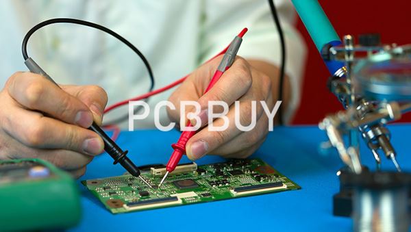
To diagnose PCB issues effectively, engineers rely on specialized tools:
|
Tool |
Purpose |
Example Usage |
|
Multimeter |
Measures voltage, resistance, continuity |
Checking for open/short circuits |
|
Oscilloscope |
Analyzes signal integrity and noise |
Debugging communication protocols |
|
Thermal Camera |
Detects overheating components |
Identifying thermal hotspots |
|
LCR Meter |
Measures inductance, capacitance, resistance |
Testing passive components |
|
Microscope |
Inspects solder joints and tiny components |
Detecting micro-cracks or poor soldering |
3. Step-by-Step PCB Troubleshooting Process
3.1 Visual Inspection (First Step)
Before using instruments, conduct a thorough visual check:
Look for:
- Burnt or discolored components.
- Cracked traces or lifted pads.
- Poor solder joints (cold solder, bridging).
Data Insight: Studies show that ~30% of PCB failures are detectable via visual inspection alone (Source: IPC-A-610).
3.2 Power Supply Testing
- Use a multimeter to verify voltage levels at key test points.
- Check for:
- Voltage drops (indicating high resistance).
- Short circuits (near-zero resistance between power and ground).
Example: A 5V rail measuring 4.2V suggests a faulty regulator or excessive load.
3.3 Signal Tracing & Oscilloscope Analysis
- Probe critical signals (clock, data lines) to ensure proper waveform shape.
- Common issues:
- Signal attenuation (weak traces).
- Noise interference (poor grounding).
Data Table: Common Signal Issues
|
Issue |
Possible Cause |
Solution |
|
Signal Ringing |
Impedance mismatch |
Add termination resistors |
|
Noise Coupling |
Poor shielding or grounding |
Improve ground plane design |
|
Jitter |
Clock instability |
Replace oscillator or filter noise |
3.4 Component-Level Testing
- Passive Components (Resistors, Capacitors):
- Use an LCR meter to verify values.
- A 20% deviation** from rated value indicates failure.
- Active Components (ICs, Transistors):
- Check datasheet for expected pin voltages.
- Use a component tester for semiconductors.
3.5 Thermal Analysis
- Overheating is a leading cause of PCB failure.
- Infrared cameras can detect hotspots.
- Example: A MOSFET running at 120°C+ may need better heat dissipation.
4. Advanced Techniques: PCB Repair & Rework
4.1 Trace Repair
- Broken traces can be fixed using conductive epoxy or jumper wires.
- Best Practice: Use 30AWG wire for most repairs.
4.2 Solder Reflow & Rework
- BGA Reballing: Replacing solder balls on BGAs requires precision equipment.
- Hot Air Rework Station: For replacing SMD components.
4.3 Firmware & Software Debugging
- Some PCB issues stem from firmware bugs.
- Use a logic analyzer to monitor communication buses (I2C, SPI).
5. Preventing Future PCB Failures
|
Prevention Method |
Effectiveness |
Implementation |
|
Proper Thermal Design |
High |
Use thermal vias, heatsinks |
|
Conformal Coating |
Medium |
Protects against moisture/chemicals |
|
Design Rule Checks (DRC) |
High |
Ensures manufacturability |
Conclusion
PCB troubleshooting requires a systematic approach, combining visual inspection, electrical testing, and advanced diagnostics. By understanding common failure modes and leveraging the right tools, engineers can efficiently diagnose and repair PCB issues, ensuring long-term reliability.
References
1. IPC-A-610 – Acceptability of Electronic Assemblies
2. IEEE Std 1149.1 – Boundary-Scan Testing
3. "PCB Diagnostics & Repair," by John R. Barnes
4. NASA Electronic Parts and Packaging Program (NEPP) – Reliability Data
Industry Category


