How to Process Rigid PCB Design for Manufacturability Guide?
By:PCBBUY 11/30/2021 09:33

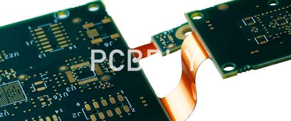
Designing a rigid flex PCB is considerably more challenging than conventional rigid PCB. However, there are good reasons why rigid flex is used in some designs, particularly one that involves fitting the board in tight spaces. Broadly speaking, a rigid flex design will closely resemble a hardboard design, with the flexible layers fully extending into the rigid areas of the board. Similarly to hardboard layouts, a rigid flex fabrication package will include Gerber layers, along with drill files, solder mask layers, nomenclature, perimeter/rout files, cover layer, etc.
If you are going to learn more about rigid PCB design, please check and read the content below for more professional knowledge in this passage. Let’s go!
What are the applications of rigid PCB?
Rigid Printed Circuit Boards offer increased circuit density and can reduces size and overall weight of the board. This is why many electronic companies in the world use these boards in several electronic devices and gadgets:
· Computers and Laptops
· Telecommunications Equipment – Mobile Phone, Tablets and other Hand Help Devices
· File server and Data storage
· Signal transmission, mobile phone repeaters, GPS
· Satellite
· Medical Equipment: Testing, X-Ray, Heart Monitor, CAT Scan
· Industrial Equipment
· Atomic and Nuclear Systems
· Military and Defense Equipment
· Automotive
· Aerospace
· Anywhere, where complex Circuitry is needed.
How to determine the structure in rigid PCB design?
Substrate Layer
The substrate layer, also referred base material, is made of fiberglass. The FR4 is mainly used as a substrate material, the most common fiberglass that provides rigidity and stiffness to the board. Phenolics and epoxies are also used as a base material, but they are not as good as FR4. However, they are less expensive and feature a unique lousy smell. The decomposition temperature of phenolics is too low, resulting in delamination of the layer if solder is placed for a long time.
Copper Layer
On the top of the substrate layer, a copper foil is laminated on the board with the help of the added amount of heat and adhesive. In everyday use, both sides of the board are laminated with copper; however, some cheap electronics come with only one layer of copper material on the board. Different boards come with different thicknesses, which are described in ounces per square foot.
Solder Mask Layer
Solder Mask Layer houses above the copper layer. This layer is added on the board to add insulation on the copper layer to avoid any damage if any conduction material is touched with the copper layer.
Silkscreen Layer
The silkscreen layer is located above the solder mask layer. It is used to add characters or symbols on the board to understand the board better. White color is mainly used for silkscreen. However, other colors are also available, including grey, red, black, and yellow.

How to process rigid PCB design?
When design multilayer rigid circuit boards, always begin with an even number of layers. The thickness of the dielectric used for the board depends on the type of materials, the dimensions, and the tolerances needed for the application. Good PCB design establishes a lay-up that balances according to the z-axis of the board. Having a balance of dielectric thickness per layer, copper thickness per layer, copper distribution, and the location of signal, ground, and power layers ensures that the board will meet bow or twist specifications.
Design for Manufacturability (DFM) requires teams to consider critical features of the design. Those features include the layer stack-up, the dielectric spacing, the drill chart, the board outline dimensions, any impedance requirements, and instructions for blind and buried vias. Decisions about each of these features can affect the design of another feature. It is important that the drawing your team submits to the fabricator describes any electrical characteristics that impact the manufacture of the board.
What is the future of flexible PCB?
There are many new designs being manufactured with substantially higher flex layer counts. Some more prevalent designs include those with blind and buried via structures, integrated ZIF connections, and even designs with components mounted into both the flexible areas and the rigid sections.
Some rigid-flex printed circuit board (PCB) designs may have flex areas that require shielding for Electromagnetic Interference (EMI) or Radio Frequency (RF) considerations. There are also designs that have varying thicknesses between the different rigid areas as well as asymmetrical constructions.
Industry Category


