How to Process Wave Soldering in PCB Manufacturing?
By:PCBBUY 04/26/2024 18:01

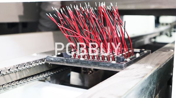
Wave Soldering is the process of soldering through-hole components onto a PCB board by passing the exposed leads of the components placed on a board over a wave of molten solder. The solder wave flows under the PCB board and applies solder to the leads of components placed on the PCB board. It is primarily used for soldering through-hole components on printed circuit boards, and it is not typically used for soldering surface mount components. If you need to solder surface mount components on a PCB, other soldering processes such as reflow soldering can be utilized.
Wave soldering was developed in 1956. At the time most components were soldered by hand which was very tedious and time consuming. The idea to pass a PCB product over a wave of molten solder seemed like a good one, and worked well as most/all components at the time were through-hole components with very long leads.
What Are the 4 Main Steps Wave Soldering Process of PCB?
Step 1: Applying Flux
Solder flux is a chemical cleaning agent used when soldering electronic components onto printed circuit boards. It is applied to the board to help avoid oxidation of the copper traces when exposed to air. It is a very important process that is required to ensure that the PCB board operates in a reliable and consistent manner. In the case of wave soldering, Flux is applied to the bottom of the board before the PCB is sent through solder wave.
No matter which method is used to manufacture the printed circuit board, it should be pre-coated with flux before welding to improve their weldability and storage to prevent oxidation during storage.
1. Flux coating method and device
The flux must be applied to the underside of the printed circuit board using the most efficient and economical method possible. The flux coating should be uniform and completely cover the solder parts. If the flux is excessive, it will not only drip onto the preheater and cause a fire risk, but also cause a lot of waste and increase the workload of cleaning the printed circuit board components. However the flux is applied, excess flux should be removed from the printed circuit board passing through the flux tank using an air knife or adjustable brush applicator. The methods of applying flux are crest, foam, brush, spray, or dip. Among them, the wave and foam coating methods are the most common.
(1) Foam flux coating device
Foam flux coating device is composed of a liquid storage tank and a long nozzle above the liquid surface. Compressed air flux is used to form a foam peak through the nozzle of the spray port. Compressed air causes the foam peak to rush out of the spray port and meet the lower surface of the welded part.
In order to prevent the foam flux from being polluted by oil and water in the gas path, filters and oil-water separators should be installed on the gas path. The pressure in the air path should be adjustable to control the air pressure and flow through the nozzle. There should also be a needle valve in the gas path, which can precisely adjust the flow rate to control the flatness of the foam peak. Using a foam flux coating device, the printed circuit board surface can be coated with a thin and uniform layer of flux. This device is more effective when the part to be welded has a large number of metallization holes
(2) Wave welding flux coating device
The wave welding flux coating device consists of a pump and a nozzle similar to the foam flux coating device. In this device, flux is sprayed through a nozzle to form a stable flux crest. Parts that need to be coated with flux can pass through the crest tip. Although this method cannot strictly control the amount of flux coated on the printed circuit board, it is suitable for mass production
(3) Flux spraying method
Flux spraying method is another method of coating flux on the surface of the printed circuit board. Its advantage is that it can accurately control the flux amount, uniformity and position. However, this method requires frequent maintenance, and the additives used should be made of volatile solvents
Brush coating and dip coating of flux Brush coating and dip coating technology is quite common technology, but this technology is not suitable for high-speed or mass production.
2. Maintenance of flux coating device
To ensure the performance of flux, it is necessary to maintain the flux coating device frequently. As mentioned earlier, the flux contains volatile deep agents, such as ethyl alcohol, etc., which should be diluted regularly to compensate for the evaporation of the solvent. The most convenient way to do this is to monitor the relative densitometer. The methods of filling the flux tank with flux are:
1) Dilute the flux in the flux tank with words, and then determine the density, the density value can generally be found in the school manual.
2) Add a newly prepared flux to the flux tank so that it reaches a certain height. It is important to replace the flux periodically and to completely empty the flux tank before filling it with new flux to minimize the containment effect in contaminants. It's also a very inexpensive method of preventive maintenance. According to different production parts, a replacement can be arranged after ten hours of work. All parts in the flux coating unit are made of acid-resistant materials, usually stainless steel or polypropylene
Step 2: Preheat
Once flux has been applied to the PCB. It is important to heat the underside of the board to a temperature of about 80 – 100 degrees Celsius. This allows any solvents present in the flux to evaporate. The flux applied using any method, is mixed with a solvent to make the application process easier, as the solvent reduces the viscosity of the flux. The flux without the solvent is a very sticky substance. This solvent is usually some volatile organic compound, which is flammable. This requires the removal of the solvent before the underside of the board comes into contact with the very hot solder wave. This is why the entire board is put through a preheating stage so as to minimize the chances of the PCB manufacturing setting itself on fire.
During the pre-heat phase, the fluxed board is passed over an array of infra-red heaters. These heaters have a heat-reflecting panel behind them. A gentle gust of air is blown between the boards and the heaters. This increases the rate of removal of solvent laden air. The heat-reflecting panel behind the heater not only reflects heat but also conserves thermal energy by reducing the temperature differential between the under-side and the top of the board.
1. Purpose of preheating
When welding, before the flux plays a role, the flux must be preheated to the activation temperature in order to react, if the material is heated to the activation temperature by the peak, then it is necessary to extend the time direction of the workpiece staying in the wave peak. A more satisfactory method is to heat the printed circuit board to the activation temperature before the piece enters the wave crest. When the workpiece reaches the peak of the solder wave, most of the flux probing material is still with the "fragrance." Some organic acid fluxes contain water, which is also a relatively volatile component. If the printed circuit board is solder in this state, the heat of the solder tank will cause the agent to volatilize rapidly, causing spatter and porosity of the solder joint. Preheating the printed circuit board removes excess volatile matter, thereby eliminating potential problems in wave solder applications. If the inner flux contains water, the preheating temperature must be higher than the temperature required if the solvent contains more volatile solvents (such as ethanol).
Preheating is to gradually increase the temperature of the components, so that the thermal impact of tin welding is minimized, and the lake curvature of the printed circuit board is minimized, which alleviates the thermal stress, so as not to affect the mechanical flatness of the printed circuit board. Preheating also minimizes the risk of damage to the thermal element.
2. Type of preheater
Radiant preheater can also be widely used preheater there are two main types: radiant preheater and positive displacement preheater step is divided into two types: long electric bar type and flat plate radiant source type.
(1) Radiant preheater
The heat transfer of radiant preheater is almost entirely dependent on thermal radiation. The temperature on the lower side of the printed circuit board is controlled by the heater temperature and the distance between the heater and the lower side of the printed circuit board. To increase thermal efficiency, the heating rod system is equipped with reflectors that concentrate the heat beneath the printed circuit board. The reflector substrate has aluminum foil, which can be adjusted and changed regularly. The flat type heater is located under the heat transfer unit, very close to the printed circuit board surface, which greatly improves the heat transfer efficiency between them. If flux drips onto the flat type heater, it must be removed regularly to prevent fire
(2) Positive displacement preheated
The positive displacement preheated is used to preheat controllable air through the lower side of the printed circuit board and maintain the efficiency of the heater. The method mainly relies on conduction and convection, and the airflow pressure helps to quickly blow away the solvent vapor under the printed circuit board. When used for printed circuit boards with metallized holes in positive displacement repeaters, positive displacement heaters should be preferred. Because the inside of the hole is often spread in a straight line by the radiation heat source, there is an objective shield, especially when it is used for multi-layer printed circuit boards. In many cases, the two methods are used simultaneously, first with a positive displacement preheater to remove excess solvent, and then with a flat-panel radiant heater to maintain the appropriate temperature
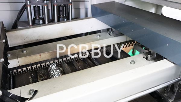
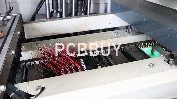
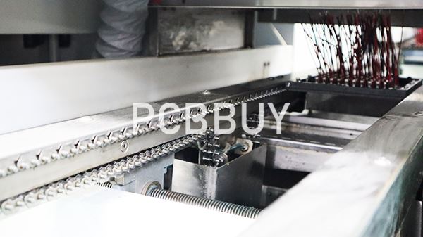
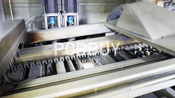
Step 3: The Solder Wave
The Printed Circuit Board is then passed through a Solder Wave. To ensure a good connection, molten solder must impact the board with maximal kinetic energy. This can be achieved when the solder wave meets the leads of the through hole components just as it is about to crest. The crest of a wave is the highest point of it.
The solder wave covers the leads of all the through hole components and connects them to the PCB.
A Solder-wave is produced by forcing molten solder-upwards through a vertical conduit. This wave of molten solder eminates from a vertical conduit, which is called a wave-nozzle. This wave-nozzle is made of narrow slots arranged at right angles to each other. An axial impeller, driven by a variable speed motor is used to drive the solder upwards.
The wave is created by melting solder ingots in a wave tank. The depot of molten solder is maintained at a temperature of about 250 degree Celsius. This has been universally accepted as the standard temperature for maintaining molten solder. If any new type of solder is being used, the temperature of the solder bath would have to change, this is because the efficiency of the a flux is strongly temperature dependent.
Step 4: Cool down
After the PCB passes over the molten solder wave, the board needs to cool down so that the solder joints can be formed. It is important to maintain a gradual temperature gradient when cooling the PCB after the wave soldering process. The temperature gradient for cooling is selected such that sudden solidification of the solder joints do not crack. This cooling rate/gradient should be selected to reduce thermo-mechanical forces generated on the board due to temperature differentials. This even cooling may be achieved by circulating cold air with zero oxygen content. This colder air must also follow a gradient of cooling proportional to the gradient of cooling which has to be induced on the board and the components on it.
Wave soldering was a very celebrated process at the time of its invention. This was due to high throughput, volume capabilities of this process. However, over time, as technology advanced and components / boards became smaller, surface mount components started to replace Thru-Hole components. This resulted in the need for different soldering processes such as reflow soldering.
What Are the Essential Advantages of Wave Soldering?
To understand the advantages of wave soldering, it is necessary to examine the alternate soldering technology in wide adoption: reflow soldering. Reflow soldering functions by heating the air in an oven to melt the solder paste pre-applied to the pads/pins before beginning the rest of the process. It’s a more targeted method of soldering than wave soldering, which simply applies solder over the bottom of the board as it passes over the molten wave. Overall, the reflow process exhibits a reduced thermal shock compared to wave soldering.
There are a few key advantages to wave soldering over reflow:
Mass production - Reflow is unable to compare to the speed of wave soldering for anything but the smallest production lots.
Cost scaling - As an outgrowth of its comparative speed advantage, wave soldering is far more affordable on a per-board basis than reflow.
Through-hole components - Wave soldering is the only way to solder through-hole components. While many components can be replaced with an SMD package, many power components still exist in a through-hole configuration, which endears wave soldering to a large market of boards.
Reference
He Wei, PCB Basic Electrical Information Science and Technology, China Machine Press,221-226
Industry Category


