How to Reduce Crosstalk in PCB through 5 Primary Factors?
By:PCBBUY 11/26/2021 09:24

Crosstalk is generally specified as a percentage of the signal that appears on the victim line, relative to the aggressor line. It can also be expressed in terms of dB below the driven line level. NEXT varies with the frequency of the transmission since higher frequencies create more interference.
In this passage, we will provide you everything about the crosstalk in PCB. If you are looking for more about the information of crosstalk in PCB, please check and read the content below.
1. What are the best practices of crosstalk in PCB?
The best way to eliminate crosstalk is to exploit the very parallelism that leads to its creation by closely coupling the return path to ground to your high-speed signals. Since the return path is equal in magnitude but opposite in direction, the fields cancel out and reduce crosstalk.
Another way to ensure signal integrity is to use differential signaling, where two voltage lines equal in magnitude but opposite in polarity are used to create a single high-speed data signal. Since the actual data signal is taken as a difference between the voltages of the two voltage lines at the receiver, and because electromagnetic noise tends to affect both lines equally, the signal itself remains perceptible even in the presence of external noise.
2. What are the issues of PCB crosstalk?
Too much activity in a circuit board can make the transmission of a signal difficult. Think of two traces on a circuit board running together side-by-side. If the signal of one trace is “louder” with more amplitude than the signal of the other, it could over-power that other trace. And just as it can be difficult in a noisy room to keep your own thoughts straight when trying to speak, the “victim” trace on a PCB will be similarly influenced by the louder signal. The problem then is that the victim signal will start behaving like the aggressor signal instead of behaving the way that it is supposed to.
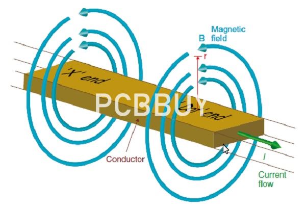
Crosstalk is defined as the unintentional electromagnetic coupling between traces on a printed circuit board. The overpowering of one signal in a trace by another one is the result of this coupling even though the two traces are not in physical contact with each other. This can happen on a PCB that has acceptable trace spacing for manufacturing but where the spacing is not acceptable for crosstalk.

3. How to reduce PCB crosstalk?
You’ve got a great ally with you these days when working to reduce and eliminate areas of crosstalk on your circuit board, and that is the functionality in your PCB design tools. At one point, design tools were very minimal in what they could help you with, but that is no longer the case.
You can set up a vast array of design rules to specify clearances between traces and from traces to other objects on the board. You can even set up different values of clearances depending on specific nets or areas where those nets are being routed through. This will help you immensely to set your design up so as to avoid situations where crosstalk could potentially develop.
Design tools also have specific functions for routing differential pairs at specific widths and clearances, and you can set up trace lengths as well as rules to match specific trace lengths to each other. You also have the ability to specify which layers of the board certain nets can be routed on and what the preferred direction of traces on those layers should be. There are also crosstalk calculators available to you as well as other simulation and analysis tools. The design tools that we have available to us today contain all kinds of design constraint features that can help with problems like crosstalk, we just have to put them to work.
4. How to use tools to remove PCB crosstalk?
PCB design tools have a lot of functionality built into them to help you to avoid crosstalk in your designs. Circuit board layer rules will help you to avoid broadside coupling by specifying routing directions, and creating microstrip stackups. With net class rules, you will be able to assign greater trace spacing to groups of nets that are more susceptible to crosstalk. Diff pair routers will route your differential pairs together as an actual pair instead of routing them individually. This will maintain the required spacing of the differential pair traces to each other and to other nets in order to avoid crosstalk.
5. How is crosstalk minimized in HDI substrates?
Crosstalk in HDI substrates is reduced by the shorter coupled lengths and by the lower dielectric constant by as much as 50 percent. Other factors that can limit crosstalk in HDI substrate include,
· Use of lower Dk materials.
· The lower dielectric constant of the HDI PCB material system may allow a board to shrink up to 28 percent.
· The thinner the distance to the reference plane, the lower the near-end crosstalk will be.
HDI miniaturization provides shorter interconnect lengths. If a lower dielectric constant material is used, then crosstalk in HDI substrates can be reduced. Eric Bogatin, Signal Integrity Evangelist at Teledyne LeCroy, provides the following example: “A typical line-width in HDI technology is 3 mils (75 microns). The figure below shows the characteristic impedance of 3-mil-wide traces for various dielectric thicknesses.
The dielectric thickness will be less for a lower dielectric constant. This means a lower dielectric constant material system will either result in less crosstalk for the same spacing, or the traces can be moved closer together and have the same amount of crosstalk.”
Industry Category


