How to Reduce Electromagnetic Interference in PCB?
By:PCBBUY 03/12/2024 15:52

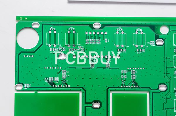
In a PCB, the ground plane is there to provide a 0 volt reference line to the power supply ground terminal for the return path of a circuit. Unlike the basin, however, when “ripples” are made, noise is produced, dipoles can form and the entire board can become an antenna. This is why the ground plane, that copper foil layer in your PCB, takes up as much of the cross-sectional area of the board as possible.
Do you know the methods of reducing electromagnetic interference in PCB? If you are searching more about reducing electromagnetic interference in PCB, please check and read the content below.
If you want to order PCB product, please check and custom your order online.
What are EMI and EMC in a PCB?
Electromagnetic compatibility (EMC) is the ability of an electronic system to operate within an electromagnetic environment satisfactorily without generating intolerable EMI (electromagnetic interference) in nearby devices/systems. EMC ensures that the system must perform as intended under the defined safety measures.
EMI is an electromagnetic disturbance, where energy is transmitted through radiation/conduction from one electronic device to another and corrupts the signal quality causing malfunctioning. EMI focuses on the testing requirements and interference between the neighboring equipment. It can occur in any frequency range, say anything more than DC. Typically, it happens above 50MHz. Read understanding signal integrity in PCBs.
Whenever a device deviates from the defined standards, EMC/EMI dominates the system performance. So, it is vital to control EMI during the initial phase of the PCB design. Controlling EMI in later production stages can be risky in cost terms. For EMC-friendly board designing, your primary concern should be on component selection, circuit design, and PCB layout design. To be market-ready, your product has to pass the prescribed EMI/EMC standards.
Why to avoid electromagnetic interference?
Sources of electromagnetic interference are all around us, and we can categorize them in several ways:
Source
Human-made EMI arises from electronic circuits. Naturally occurring EMI, on the other hand, can arise from environmental factors like cosmic noise and lightning.
Duration
Continuous interference is an EMI source that emits a constant signal, which most often appears as background noise. Impulse interference is intermittent, usually caused by switching systems, lightning and other non-constant sources.
Bandwidth
Narrowband signals like those used by radio can encounter interference from oscillators and transmitters, though these sources only affect certain parts of the spectrum intermittently. Broadband interference affects high-data signals like TV and can come from many sources, including arc welders and solar noise.
Whether human-made or environmental, EMI can be both costly and dangerous. It can disrupt communication channels and sensitive devices. EMI is a notable concern in the medical field, where wirelesses device usage is on the rise. Unfortunately, EMI can affect the functionality of medical equipment like ventilators, ECG monitors, cardiac monitors and defibrillators. In other industries, EMI can disrupt sensors and navigational systems. The result in all cases is a disturbance of equipment that may be responsible for the health and safety of its users.
How to Reduce Electromagnetic Interference in PCB?
PCB board design techniques for electromagnetic interference (EMI)
There are many solutions to the EMI problem in today's PCB board design techniques, such as EMI suppression coatings, suitable EMI suppression parts, and EMI simulation designs. The above film describes how to reduce EMI. Now briefly explain these tips.
· Common mode EMI interference sources (such as the voltage drop formed by the transient voltage formed in the power busbar across the inductor of the decoupling path)
· With low-value inductors in the power plane, the transients synthesized by the inductors are reduced and common-mode EMI is reduced.
· Reduce the length of the power layer to IC power pin connections.
· Use 3-6 mil PCB layer spacing and FR4 dielectric material.
Electromagnetic shielding
· Try to place the signal traces on the same PCB layer and close to the power or ground plane.
· The power plane should be as close as possible to the ground plane
The layout of the parts (different layouts will affect the circuit's interference and anti-interference ability)
· Block processing according to different functions in the circuit (such as demodulation circuit, high-frequency amplifier circuit and mixing circuit, etc.), in which the strong and weak electrical signals are separated, and the digital and analog signal circuits are separated.
· The filter network of each part of the circuit must be connected nearby, which not only reduces the spokes, but also improves the anti-interference ability of the circuit and reduces the chance of interference.
· Parts that are susceptible to interference should be avoided as much as possible in the layout, such as CPU interference on the data processing board.
Industry Category


