How to Reduce Parasitic Capacitance in PCB Layout?
By:PCBBUY 03/07/2022 10:07

Parasitic capacitance or stray capacitance is the result of a virtual capacitor formed between two traces separated by a dielectric. It occurs due to the potential difference generated when the current-carrying traces run in close proximity. To learn more, read the role of trace current capacity in PCB design. This effect is even possible if the conductors are appropriately insulated. It is not possible to avoid parasitic capacitance since no electrical circuit is ideal.
Do you know how to reduce parasitic capacitance in PCB layout? If you are searching for more information about parasitic capacitance in PCB, please check and read the content below for more knowledge.
What is the function of parasitic capacitance in PCB layout?
Parasitic capacitance is likely to be present in a circuit, and for low-frequency designs, it is unlikely to cause any major issues. However, parasitic capacitance can be a major problem when in a high-speed design.
As the frequency increases, the behavior of the capacitor changes, and it eventually acts as a short circuit. You can expect the same from parasitic capacitance when high-speed signals are running through one of the elements.
In an amplifier design, parasitic capacitance that forms between the input and output can result in unwanted feedback. The usually open-circuit path becomes conductive when operating at high frequency and causes undesirable oscillation or parasitic oscillation in the amplifier circuit.
Parasitic capacitance can be troublesome for two adjacent conductors. When one of the conductors carries a high-frequency signal, it can introduce crosstalk to the other conductor. Higher parasitic capacitance leads to higher EMI noise.
Not only does parasitic capacitance create interference, but it can also affect the integrity of the signal itself. For example, parasitic capacitance can build up between a conductor and the ground plane. At high frequency, both elements behave toward a short circuit and will alter the signal on the conductor.

How to calculate parasitic capacitance in PCB?
Parasitic capacitance is an inherent property of the conductors. It is the storage of per unit change in electric potential. The parasitic capacitance is calculated as C= q/v. Where C is the capacitance in farads, v is the voltage in volts, and q is the charge in coulombs.
· For a constant electrical signal that does not change over time, dv/dt = 0 which means, no change in potential; hence i =0.
· If there is a capacitor in the circuit loop, dv/dt will converge to a fixed value, i.e., change in potential, resulting in a current flow; hence i ≠ 0.
Trace capacitance calculation
The capacitance of a parallel plate capacitor is given by C= (kA/11.3d)pF. Where C is capacitance, A is the plate area in cm2, k is the relative dielectric constant of board material, and d is the distance between the plates in cm.
How to reduce the effects of PCB stray capacitance?
Remove inner layer ground plane
As ground planes can increase capacitance with adjacent conductors due to proximity, it can be helpful to remove an inner-layer ground plane to increase the distance which will minimize the capacitive effects. This has to be balanced against the benefits of minimizing EMI that is gained when ground planes are adjacent to signal planes.

Use a Faraday shield
A Faraday shield is a ground trace or plane that is placed between two traces to minimize the capacitive effects between them and it, like other shielding structures, is effective at minimizing stray capacitance.
Increase space between adjacent traces
Another effective mitigation technique is to increase the spacing between adjacent traces. As capacitance decreases with distance this is a very good approach when it can be applied.
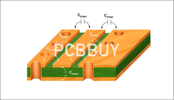
Minimize the use of vias
Vias are the key elements that make compact, complex PCBAs possible. However, excessive use can increase your parasitic capacitance issues; such as stray capacitance. This PTH coupling can be reduced by eliminating annular rings around vias on layers where there is no connection and minimizing the number of vias from components; such as BGAs.
Industry Category


