How to Reverse Engineer Multilayer PCB of 6 Aspects in Manufacturing Process?
By:PCBBUY 10/13/2021 10:00

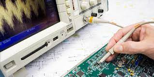
Do you know what reverse engineer is? It is the process of disassembling and analyzing a physical product to generate documentation, remanufactures, and determines how it was designed and operates. Often the documentation even allows a customer to improve their product to surpass competitors.
If you are curious about the detailed information about reverse engineer of multilayer PCB, please check and read the content in this passage for more information. Let’s get it!

1. What is the basic definition of Multilayer PCB reverse engineer?
In addition to our PCB Engineering capabilities we also provide a service to reproduce PCB artworks for old or obsolete printed circuit boards where the original is no longer available. This technique involves scanning the printed circuit board and accurately recreating the track work, component idents, resists and NC drilling information in our VCAM software. The customer can then order replacement printed circuit boards as required.
2. What is process of Multilayer PCB reverse engineering?
· Assign reference designations to unmarked components before starting PCB reverse engineering.
· Create a Component level BOM.
· Design -Identify the system’s components and their interrelationships.
· Components Placement & Mechanical.
· XY locations of Connectors, LED, Switches etc.
· Board mechanical Mounting holes & any special cuts on Boards, Board size etc.
· Download datasheets, application notes, and architecture information.
· Create net list.
· Make the Schematic Drawing and PCB Layout.
3. What are the applications of multilayer PCB reverse engineer?
· Circuit extraction and reverse engineering of obsolete parts
· Identifying patent infringement
· Building a “known parts” database for counterfeit screening
· Gathering competitive intelligence in preparation for new product launches
4. What are the considerations during multilayer PCB reverse engineer?
Becoming a PCB reverse engineer isn’t necessarily simple. But there are three main steps you need to take to achieve a functioning PCB without documentation or support.

Reverse Bound Constructing
To begin, you need accurate—and well-lit—images of both sides of your PCB. With these two images, you can create a layout for developing a schematic. With a basic board, you can use graph paper to draw the layout. Use symbols for each component and work carefully to capture the proper scale.
For more complex PCBs, using pencil and paper quickly becomes confusing. However, if you can create a line drawing for a relatively detailed PCB, you can skip image editing and color switching and go straight to preparing a schematic.
Using photographs is time-consuming, but it’s a necessary step for more complex layouts. Good lighting and a quality camera (whether digital or smart phone) will help make the process easier. You need a photograph of both sides of the PCB to begin.
5. What is limited liability on PCB reverse engineering?
What we guarantee for the PCB reverse engineered board is the Gerber files and BOM are identical to the original board. We will refine the files if you show us some differences brought from software bugs or due to human being errors after you review the first version of the files. After you approve the Gerber files and BOM the PCB reverse engineering is completed and we will start making the sample bare boards and, if required, then follow up by assembling the sample boards with the components from the approved BOM. Most likely, the samples are one or two boards.
6. Why we process a best PCB reverse engineering?
Reverse engineering a PCB is generally done because we want to copy the device or determine how it works. There are many reasons for doing this, both legitimate and not so legitimate.

One reason for it is that the part is obsolete and must be updated and replaced. Sometimes the original design data has been lost. Another reason is that a company is trying to copy a competitors product.
The goal is to develop the schematic and parts list that was used to design the PCB in the first place. With older circuits that are made of discrete components (transistors, resistors, etc) the process is easier. Identifying the parts on the PCB is the first step and then determining how everything is connected is the second step. Both of these can be a challenge.
Newer circuits (i.e. a smart phone) can have specialized integrated circuits and reverse engineering those is another topic. Modern PCB’s generally have a large number of layers (making the problem more difficult) while older circuits tend to have 2 to 4 layers.
A successful reverse engineering project results in a new part that can replace the older part in some piece of equipment. Or it can result in a product that will compete in the market place against the target product.
Industry Category


