How to Route PCB Traces & What Are Techniques of It?
By:PCBBUY 03/12/2022 10:10

When designing your PCB layout, there are many considerations that must be incorporated into your choices and decisions. A popular way to integrate these concerns is to adopt a design perspective that helps you organize your design choices.
In this passage we are providing all the information about PCB routing and the techniques of it, please check and read the content below ion this passage.
How to determine PCB trace impedance?
If we know the geometry of a trace and the properties of the material(s) surrounding it, how do we then calculate the trace’s impedance? In decades past we used various formulas for this. These formulas could be found in various application notes and industry standards, and they were “close enough” then to be suitable. But as requirements have become more precise, these older formulas are no longer considered reliable for the precision we now require. Our requirements became more difficult as we began to want formulas for edge-coupled differential traces, and there never have been reliable formulas for broadside-coupled differential traces.
You can change these geometric features and still retain controlled impedance as long as you change other features as necessary so the relationship between these aspects does not change and impedance remains constant.
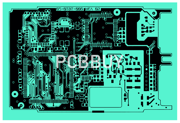
What are the considerations of PCB routing?
Constraints and rules are used in PCB design for a number of reasons. They will help you to organize your design and communicate important information between the schematic and the layout. Primarily, though, they are used to prevent manufacturing problems and to ensure the electrical performance of the circuit board. Here are some issues that constraints are designed to address:
Manufacturing Problems:
Components that are placed too close to each other or oriented incorrectly may be difficult to assemble or solder correctly. Additionally, auto-insertion machinery may not be able to place the parts as needed, and technicians doing manual assembly may not be able to fit their tools and solder materials into the tight areas.
Metal on the circuit board that is too close to other metal objects may also cause problems during the manufacturing process. Solder slivers can form, causing intermittent shorts, which are difficult to find and correct. Solder can also bridge between traces or pads causing direct shorts.
Electrical Performance:
Traces used to conduct power that aren’t wide enough may be inadequate for the amount of current that they are carrying. Some traces also must have exact widths to control their impedance. Other traces need to be routed to a specific length or to match the length of similar nets. Differential pairs must be perfectly routed side-by-side.
It used to be that you could take a PCB design, throw it into the auto-router, and end up with a completely routed board that worked perfectly. That is no longer the case. Without the proper care in trace routing widths, spacing, lengths, and topologies, you may end up with a plethora of signal integrity problems.

What are the useful PCB routing techniques?
While a successful PCB trace routing strategy relies on a solid schematic and good component placement, like most things it also takes experience. To put it simply, the more you route, the better you are. There are however some features in your PCB design software that can provide a lot of help with trace routing including:
· Automatic routing features such as batch auto-routing and auto-interactive routers can help you to create your traces much faster than you can manually. The key is to understand how they work and learn the routing scenarios where they perform best.
· Editing features that control options (like how much of a trace to rip up when deleting them). These are often user-configurable and can be set to delete the entire line or just to a certain segment.
· Push and shove features that will move existing traces and vias out of the way when routing in new traces.
· Display features that control the color of different layers, or highlight specific nets.

In addition to the functionality of the CAD tools that can help, remember that trace routing is also an artistic task. Give yourself the freedom to be creative in how you route your boards. Don’t be afraid to rip up and re-route, or to move large portions of circuitry to create a better routing pattern. While you are at it, please use those design rules and constraints with your system’s online checking that you set up before the layout. Spending a little extra time beforehand to correctly set up the design constraints could end up saving you hours and hours of redesign to correct unexpected layout errors.
Industry Category


