How to Shield PCB through 5 Effective Methods in PCB Design?
By:PCBBUY 12/17/2021 09:28

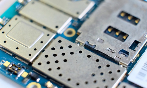
Shielding a design requires that it be encapsulated on both sides with a layer of material that acts as a barrier to the absorption or radiation of EMI. These layers are connected to ground so that any EMI is harmlessly dissipated.
Do you the methods of PCB shield? Are you curious about PCB shield? If you are searching for PCB shield information, please check and read the content in this passage for more professional knowledge.

1. What are the main types of PCB shield?
PCB RF Shielding
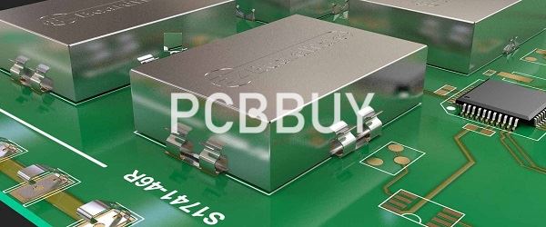
Electromagnetic Interference shielding or EMI shielding that impedes radio frequencies and electromagnetic radiation is called RF shielding. This type of shielding reduces the coupling of radio waves, electromagnetic fields and electrostatic. A conductive enclosure used to block electrostatic fields is also known as a Faraday cage.
Arduino Shielding
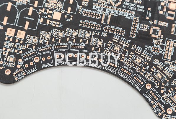
The Arduino EMI PCB shield is a board that can be mounted on top of the Arduino board. Its shield pins are inserted into the sockets located down both sides of the Arduino board. Arduino has a large, range of shields designed for prototyping.
2. What is the working principle of PCB shield?
The main purpose of effective EMC Shielding is to prevent electromagnetic interference (EMI) or radio frequency interference (RFI) from impacting sensitive electronics. This is achieved by using a metallic screen to absorb the electromagnetic interference that is being transmitted through the air. The shield effect is based on a principle used in a Faraday cage – the metallic screen completely surrounds either the sensitive electronics or the transmitting electronics. The screen absorbs the transmitted signals, and causes a current within the body of the screen. This current is absorbed by a ground connection, or a virtual ground plane.
By absorbing these transmitted signals before they reach the sensitive circuitry, the protected signal is kept clean of electromagnetic interference, maximizing shielding effectiveness.
A good example in every person’s pocket is the smart phone. It is essential that EMC shielding is used to protect the sensitive electronics in the device that make it process and display information from the phone’s transmitter.
3. How to process PCB shield during design?
If you remember your basic electromagnetics classes, you should know that a grounded metal plate greatly attenuates electromagnetic fields. Stray electric fields, including RF fields, can be effectively shielded using a metal enclosure that surrounds sensitive components. When various components are separated into different enclosures, the electromagnetic shielding also prevents interference between components.
Once the EMI shielding is grounded, it can provide a conducting plane for ESD, RF fields, internal fields, and noise carried on the cables that enter and exit the enclosure. The shielding must provide a low impedance path for external RF sources to reach ground reference point in order to quickly dissipate any currents induced by stray fields.

4. What are the techniques of processing PCB shield?
There are additional considerations that must be factored in when choosing a shield method and material.
Bend Requirements
Each shielding method adds different amounts to the overall thickness of the flexible circuit. As the minimum bend capability is a function of the thickness, it will reduce or limit the bend capabilities of a design. The minimum bend radius and type of bend requirement of shielded designs needs to be accurately defined and reviewed as part of the design and material selection process.
The type of bend requirement static or dynamic, places further constraints. A dynamic bend flex PCB application has a much larger minimum bend capability than that of a static bend design.
Controlled Impedance
Controlled impedance signal requirements place further limitations on the shielding method that can be used. The shield(s) require electrical characteristics that satisfy both the EMI requirements as well as perform as reference planes to achieve the required controlled impedance values. Not all shielding methods can satisfy both.
5. What are the considerations of processing PCB shield?
How to design a board with low or absolutely zero electromagnetic interference? Well, it isn’t impossible. The below design practices will make sure you do not create antennas, which will emit electromagnetic energy. These best design practices will reduce the length and area of the potential signal return paths that may increase unwanted EM emissions. The multi-layers stack-up

Trace spacing and layout
Traces are the conductive paths that carry current from the driver to the receiver on the PCB. When these traces come across any bend or cross, they form a fully radiating antenna. Some common trace design rules are:
Ground planes
A ground with low inductance value is a crucial element during PCB designing for mitigating EMC problems. Increasing the ground area on a PCB reduces the ground inductance in the system, hence EM emission and crosstalk too. Several approaches are available when we need to connect the signals to the ground, but what is best? Before jumping to the best PCB design approach, let us discuss what is not at all acceptable? Never connect the PCB components randomly to the ground points. So, what is the recommended design approach?
Industry Category


