How to Solder PCB Trace with 5 Effective Tips in PCB Manufacturing Process?
By:PCBBUY 11/02/2021 09:28

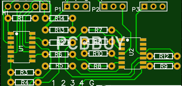
PCB trace is important for each PCB like a current, and it will spend more time and energies on fitting if make it wrong to detect or calculate the trace. What’s worse, it may lead to making mistake in the system for any device.
There are many components in the printed circuit board and you should understand which parts and materials you need as repairing or assembling the printed circuit board. As well as what kinds of functions and formulas you should take. In this passage, we are providing all the details about PCB trace. If you are curious about PCB trace, please check and read the content below.

1. What is the importance of PCB trace?
The relationship between trace width and current carrying capacity in your printed circuit boards is fairly straightforward. Specifically, a cross-sectional area of trace and temperature rise determines your current carrying capacity, with your cross-section of trace directly proportional to copper thickness and trace width.
However, this does not necessarily mean that trace carrying capacity is directly proportional to cross-sectional area. Calculating the maximum current that a trace is able to hold based solely on trace width and temperature rise is not always a simple calculation, as you may already have found. The thicker traces have been optimized for current carrying capacity and are used for peripherals or power-related functions that demand higher power, such as fans, motors, and general power delivery to lower level components.
2. How to determine PCB trace impedance?
If we know the geometry of a trace and the properties of the material(s) surrounding it, how do we then calculate the trace’s impedance? In decades past we used various formulas for this. These formulas could be found in various application notes and industry standards, and they were “close enough” then to be suitable. But as requirements have become more precise, these older formulas are no longer considered reliable for the precision we now require. Our requirements became more difficult as we began to want formulas for edge-coupled differential traces, and there never have been reliable formulas for broadside-coupled differential traces.
You can change these geometric features and still retain controlled impedance as long as you change other features as necessary so the relationship between these aspects does not change and impedance remains constant.

3. How to apply the PCB trace resistance?
Another example of how this can play out is in resistance based current sensing circuits in power systems. If the sense resistor is 1 ohm and you use the same .025mm trace, the system will measure the resistance at 1100 ohms instead of the preferred 1000 ohms. That is quite a difference, and it can lead to a weaker currency than expected or even necessary.
There do exist ways to work with the trace width that does not involve complicated calculations. These solutions can save much time, and you should consider before performing more complex calculations. You can regard these options to determine the trace width without needing to calculate the PCB trace width.
The first of these can be done by merely eyeballing the width and increasing or lower it to see what kind of circuits are connected to it properly. It will do a couple of things. First, it will increase the area of copper, giving you a bit more room for experimentation with different ohm levels. Second, it will reduce the resistance of the copper on the board. It will also allow for a bit more testing to determine a proper trace width.
4. How to solder PCB trace?
You can cut or break a PCB trace using a screwdriver, PCB scraper, and a knife. After scratching the PCB trace back and forth with the utmost care, you can remove the thin copper layer. When you perform this task, you must make sure that the surrounding traces are not damaged. So, it is always advisable to do it slowly and accurately. To cut a PCB trace vertically, it can be scratched using the corner of a screwdriver.
You can cut a circuit board trace using a knife, a milling tool, or any other device with a sharp edge. A PCB cannot be cut like paper. To remove the thin copper layer, you need to scrap a few times.
A PCB is a building block of an electronic device. Trace makes a very vital component of a circuit board. It is always advisable to have proper awareness of a printed circuit trace while repairing a circuit board. According to experienced design engineers, thickness makes a strong impact on the PCB design. It plays a very critical role in maintaining the balance of the PCB.
You should have a solid understanding about the circuit board trace current to learn more deeply about the functioning and repair of the PCB traces. Accomplished designers also know how to measure the width of PCB trace. .

5. How to calculate PCB trace width?
Let's walk through the process of calculating for a certain trace width for a power signal delivering current from one power component to a peripheral. In this example, we’ll be calculating the minimum trace width for a power-path used for a DC motor. The power-path starts at a fuse, travels through an H-bridge (a component used to manage power delivery across a DC’s motor windings), and ends at the motor’s connector. The average continuous max current demanded by the DC motor will be around 2 Amps.
Now, a PCB trace acts as a resistor and the longer and narrower the trace, the more resistance is added. If the trace isn’t properly defined, the high current could damage the trace and/or introduce significant voltage drop to the motor (resulting in a slower speed). NetC21_2 shown in Figure 3 is about 0.8” long and needs to carry 2 Amps max. If we assume some general things like a 1-ounce copper pour and ambient room-temperature during normal operation, we have what we need to calculate both the minimum trace width and expected voltage drop at that width.
Industry Category


