How to Solder Through Hole PCB during Manufacturing Process?
By:PCBBUY 12/30/2021 09:51

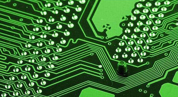
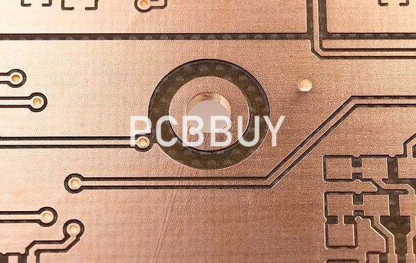
Printed Circuit Boards electrically connect electronic components through conductive pathways, tracks or signal traces that are etched onto a copper-plated sheet. The PCB board itself is made of a non-conductive substrate and has several holes drilled through it. These holes are drilled with coated, solid, tungsten carbide drill bits and are prominent in diameter. The holes are made conductive by electroplating with copper.
If you are curious about the process of Through Hole soldering on PCB, please check and read the content below for more information. You may find all the details about Through Hole soldering on PCB.

What are the advantages of Through Hole on PCB?
The origin of through hole technology (THT) can be traced to as far back as the 1950s. Through hole technology is a kind of electronic circuit construction that entails implanting leads of through hole components through holes bored into printed circuit boards (PCBs) then soldering the leads on the other side. This process is also called through hole assembly.
Point-to-point construction was the technology used in circuit construction before the arrival of through hole technology. Through hole technology was the method used to assemble components on a printed circuit board (PCB) until the emergence of surface mount technology during the late 1980s.
Benefits of Through Hole Technology
Soldering through hole components is relatively old technology. However, it is still a useful method. Through holes soldering makes the bond between the printed circuit board and the through hole components very strong. Thus, through hole soldering is an appropriate method for electronic equipment that will be subjected to mechanical stress or excess heat. Transformers are an example of such equipment.
Also, it is easy to maneuver through hole PCBs. This makes them suitable for testing and manufacturing prototypes. In addition, the holes are well spaced which allows through hole soldering by hand.
THT soldering could be cost-effective. When working with through hole PCBs you do not have to generate a different solder template every time you alter the PCB. This could help save a lot of money especially if the design undergoes a couple of spins or more before it is satisfactory. Also, tin-lead solder can be used during THT soldering. This solder is the cheapest exterior metallization.

How to process Through Hole on PCB?
Alkaline cleaning
Remove the board oil , fingerprint, oxide, dust in the hole; adjust the negative charge to positive charge for hole wall so that the colloid palladium does well in being adsorb in the post-process; it should be strict with cleaning based on guidance after unoil and test with PTH backlight.
Mircoetching
Removing the oxide of board, and roughening the board, to make sure that there is a good bonding between plated through hole layer and base copper; the new copper foil has a strong active and does well in adsorb the colloid palladium;
Pre-dip
It’s mainly in protecting the palladium slot from being polluted for the bath of pretreatment and extending the shelf life, the main ingredients of pre-dip is the same as palladium slot but except the palladium chloride, and pre-dip plays an effective role in wetting the hole wall so that the following activator enter the hole on time to be activating effectively;
Activating
The hole wall with positive charge plays an effective role in adsorb the colloidal palladium particle with negative charge to make sure that the following the averageness, continuous and compactness of plated through hole after the polarity of adjusting for pretreatment alkaline cleaning; so unoil and activating is so important for the later plated through hole. The control point of activating: specified time; normal density of stannous ion and chloride; what’s more, it’s also important for pecific gravity, acidity and temperature, so it should be controlled strictly on guidance.
Desmearing
Remove the stannous ion outside the colloidal palladium particle to expose the palladium nucleus so that plays an effective catalysis role in starting the plated through hole, it can be shown that it’s better to use the fluoroboric acid as desmearing.
PTH
Bring out the autocatalytic reaction of PTH with activating of palladium nucleus, it can be a catalyst to do the vcatalytic reaction for the new electroless copper and by-product hydrogen to keep the plated through hole. And it can be depositing a plated through hole on the board or hole wall after treating. The bath need to be normal air agitation in the process so that the soluble cupric is changing.
Industry Category


