How to Test PCB with 5 PCB Testing Techniques?
By:PCBBUY 09/14/2021 09:25

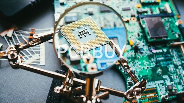
As the essential part of part of PCB manufacturing process When PCB testing is conducted throughout the production cycle, it can help save money and prevent issues when it comes to the final production run. These tests, run on prototypes or small-scale assemblies, look most closely at potential shorts, solder joint issues and functionality, ensuring that each tested PCB will function as intended.
In this passage, we will provide 5 PCB testing techniques to finish the test process for PCB. If you are going to learn more professional knowledge, please check and read the content below.
If you want to order PCB product, please check and custom your order online.
What are the advantages of PCB testing?
Many companies see PCB testing as an absolute must due to the many advantages it provides them. Check out some of the following top advantages of PCB testing:
Increased safety
Since PCBs are often used in essential electronic technologies, their failure can cause major issues for a company’s productivity or an organization’s ability to perform essential services. A defective PCB could cause a fire, potentially putting those near it in danger.
Time savings
PCB testing in the early stages can help save time in the long run, allowing designers to identify major issues during the prototyping stage. Thorough testing enables designers to determine the root cause of each problem posed quickly and easily, making adjustments so that they can move on with production at a faster rate and reduce product lead-time.
Cost reduction
PCB testing prevents wasteful production of faulty products by using prototypes and small-scale assemblies to test the products. By completing thorough testing early in the design process, designers can prevent wasteful full-scale assemblies of faulty PCBs, ensuring that the design is as flawless as possible before it goes into production.
What are the different 5 types of PCB test?
What is In-Circuit Testing?
In-circuit testing (ICT) is a fully automated test. It’s also known as bed-of-nails testing because the method resembles a bed of nails. In ICT, the PCB is pressed down on a board of probes, and needles come up to test the circuit at predesigned access points. A certain amount of pressure is applied to see if the connections are working correctly.
In-circuit testing is the most thorough of the tests and takes the most time. Because of these factors, this test comes at a high price point. For ICT, the cost can reach more than $10,000 depending on your printed circuit board’s size and functionality.
What is Flying Probe Test?
The flying probe test (FPT) is an automated testing technique. In this technique, one or more automated robotic probes fly over the cross-section of assembled PCBs. These robotic probes perform the inspection while flying from pin to pin. In this technique, the flying probe checks the performance of mounted components.
This technique of PCB inspection is adopted for inspecting prototype PCBs and high-density PCBs. This technique is preferably chosen for small batches of PCB testing. However, this technique can also be used for high-volume PCBs batches of PCB testing, where the probe is moved across the length of the conveyor where assembled PCBs awaiting testing and inspection are placed.
What is AOI?
AOI system uses a single 2D or two 3D cameras visual input to monitor PCBs for defects. They are able to sense a variety of defects such as nodules, scratches, and stains as well as the more familiar dimensional defects such as open circuits, shorts, and thinning of the solder. AOI is very useful for the early detection of assembly issues.
The template method is more accurate, however this is time-consuming to set-up and is not suitable for prototype designs subject to changes.
What is X-Ray Inspection?
The X-Ray or AXI can detect elements that are usually hidden from view, such as internal traces & ball grid array packages with solder joints under the chip package. There are 2D & 3D AXI tests available in today’s PCB industry, with 3D offering a faster testing period.
When used alongside the production process, AXI can be a useful tool for detecting defects early on, thus allowing engineers to make process adjustments to eliminate the source of the issue. This reduces the number of boards requiring costly repairs. For small batches or prototyping, x-ray inspection of only the chip components with hidden pads is often sufficient.
Advantages:
· Can have the highest defect detection rates of common inspection methods.
· Emphasis on long-time solder joint quality, not just connections.
What is Burn-in Test?
As the name suggestions, burn-in testing is a more intense type of testing for multilayer PCBs. It’s designed to detect early failures and establish load capacity. Because of its intensity, burn-in testing can be destructive to the parts being tested.
Burn-in testing pushes power through your electronics, usually at its maximum-specified capacity. The power is run through the board continuously for 48 to 168 hours. If a board fails, it is known as an infant mortality. For military or medical applications, boards with high infant mortality are clearly not ideal.
Industry Category


