How to Test Thermal Relief Valve the PCB Manufacturing Process?
By:PCBBUY 04/18/2022 10:01

Thermal reliefs are the spooked connections from a thru-hole or surface mount pad to an area fill or plane. Their purpose is to provide a robust electrical connection from the pad to the plane while preventing the heat needed for soldering from dissipating into the metal plane. The green color represents a solid plane of copper on a circuit board in the picture below, and you can see four thermal relief connections for each outer pin. In the case of a surface-mount pin that connects to a large metal area, multiple traces may be used from the pad to the copper to accomplish the same results.
In this passage, we will focus on the thermal relief for a PCB. And if you are going to learn more information of thermal relief for a PCB, please check and read the content below in this passage for professional knowledge.
What is the Importance of PCB thermal management?
Current silicon-based components have a junction temperature between about 125°C and 200°C. However, it is necessary to avoid reaching this value, otherwise the residual life of the component will deteriorate rapidly. In fact, it is estimated that an increase in operating temperature of 20°C, due to inefficient thermal management, can reduce component life by up to 50%. High brightness LEDs, for instance, convert over 60% of the absorbed power into heat and therefore require special printed circuit boards capable of handling high temperatures without damaging the components.
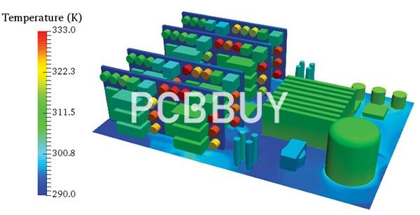
The growing popularity of wide bandgap (WBG) semiconductors, such as gallium arsenide (GaN) and silicon carbide (SiC), has allowed components to reach higher operating temperatures than silicon-based technology. This, however, has not eliminated the need for accurate thermal management, capable of evenly distribute the generated heat, avoid the formation of dangerous heat accumulation points (hot spots) and minimizing power losses. Figure 1 shows an electronic circuit subjected to thermal scanning by infrared camera: the red colored parts correspond to the points of greatest heat concentration.
What are the considerations of thermal relief for a PCB?
A board's design dictates the component connections to these broad areas of metal for necessary functionality. One other exacerbating issue is that a design's requirements typically include as much metal as possible to accommodate the PCB's electrical demands.

And, to facilitate increased current loads and enhance power integrity, power nets also require this metal. As you might imagine, this creates a dichotomy between electrical performance and standards of manufacturability. However, this is where thermal relief can provide a much-needed compromise.
What are the guidelines of thermal relief PCB?
Are you going to deal with thermal relief PCB? Then, you must know some relevant guidelines to avoid mistakes.
You have to use thermal pads while connecting your thru-hole pin to the power place, metal fill, and other bigger metals.
You must know how much power the pin can conduct. Based on this factor, you can identify the width and number of spokes. You can achieve 40 mils of spokes with 4 spokes. Each of these spokes must have a width of 10 mils.
SMT components directly soldered to the big metals must have some thermal relief between the metal and solder pad.
In a few cases, you may not be able to connect all spokes to the thermal relief pad. The congestion of thermal reliefs can result in this problem. Moreover, when the metal has very limited space, and you use thermal reliefs in the split plane, you will encounter this problem. You have to ensure that the chosen software has its own rules to detect minimum connections of thermal reliefs.
It is essential to know about the terminologies related to components and pads.
Termination and termination width– Termination refers to a metallization band present at the chip component’s end. The termination’s width is about the dimension across the chosen component.
Tolerance– It is about how much pad is used under your component.
Overlap– The component termination covers a pad surface known as overlap. The overlap has a length that includes tolerance.
How to design thermal relief for a PCB?
In this step, you can notice a difference in temperature across the circuit board. The temperature difference can be up to 95°C.

The process for rework is about the correction of errors found during reflow. Those errors comprise some misaligned parts and unacceptable connections. The overall process for soldering can increase the board temperature.
You will achieve success in the board manufacturing process based on the board materials’ potential to endure temperature for soldering activities. But, the potential is not simply about the material properties. It is related to the PCB thermal relief design for your manufacturing purposes. You can notice some issues associated with-
· Soldering components parts – Based on the solder type, the temperature level at the joints of these components can be different.
· Thermal relief– It denotes the heat dissipation path while dealing with PCB assembly.
· Thermal stress – It is the high amount of heat, which causes stress on your board.
· Thus, you must have knowledge about these rules and guidelines to work on the design of your thermal reliefs. You can rely on the best manufacturers to get other relevant information.
Industry Category


