How to Understand Applications of Multilayer PCB?
By:PCBBUY 02/24/2025 15:11
Introduction
Multilayer Printed Circuit Boards (PCBs) have become a cornerstone in the development of modern electronics. As the demand for more compact, efficient, and high-performance electronic devices continues to grow, multilayer PCBs offer a solution by providing enhanced functionality and reliability. This article explores the applications of multilayer PCBs, delving into their principles, necessary chemical processes, and the advantages they offer over single and double-layer PCBs. We will also provide detailed data and comparative tables to illustrate the efficacy and potential of multilayer PCBs in various industries.
What Are Principles of Multilayer PCBs?
Understanding Multilayer PCBs
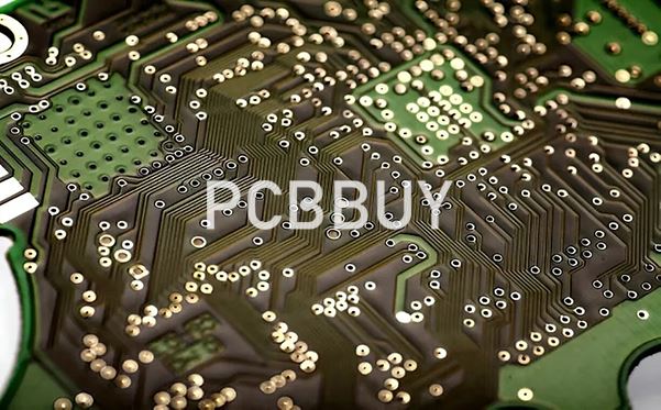
Multilayer PCBs consist of multiple layers of conductive and insulating materials laminated together to form a single board. These layers are interconnected through vias, which are small holes filled with conductive material. The complexity and number of layers can vary, typically ranging from 4 to 12 layers, but can extend to 50 or more in advanced applications.
Layer Composition and Materials
The layers in a multilayer PCB are composed of the following materials:
1. Conductive Layers: Typically made of copper, these layers form the electrical pathways.
2. Insulating Layers: Usually made of epoxy resin reinforced with fiberglass (FR-4), these layers separate the conductive layers.
3. Prepreg: A semi-cured material that bonds the layers together during the lamination process.
Manufacturing Process
The manufacturing of multilayer PCBs involves several critical steps:
1. Layer Preparation: Each conductive layer is etched to form the desired circuit pattern.
2. Lamination: The layers are stacked and bonded together under heat and pressure.
3. Drilling: Vias are drilled to create interconnections between layers.
4. Plating: The vias are plated with conductive material to ensure electrical connectivity.
5. Final Etching: The outer layers are etched to finalize the circuit patterns.
6. Surface Finishing: The board is coated with a protective layer to prevent oxidation and enhance solderability.
What Are Chemical Processes in Multilayer PCB Manufacturing?
Several chemical processes are integral to the manufacturing of multilayer PCBs:
1. Etching: The removal of unwanted copper from the conductive layers using chemical etchants such as ferric chloride or ammonium persulfate. The reaction can be represented as:

2. Electroplating: The deposition of a thin layer of conductive material (e.g., copper) onto the vias to ensure electrical connectivity. The reaction can be represented as:

3. Lamination: The bonding of layers using prepreg, which undergoes polymerization under heat and pressure. The reaction can be represented as:

What Are Advantages of Multilayer PCBs?
Enhanced Functionality and Complexity
Multilayer PCBs allow for more complex and dense circuit designs, enabling the integration of advanced functionalities in a compact form factor. This is particularly beneficial for high-performance applications such as smartphones, computers, and medical devices.

Improved Signal Integrity
The multiple layers in a multilayer PCB provide better signal integrity by reducing electromagnetic interference (EMI) and crosstalk. This is achieved through the use of dedicated ground and power planes, which shield the signal layers.
Higher Reliability and Durability
Multilayer PCBs are more reliable and durable due to the robust lamination process and the use of high-quality materials. They are less prone to mechanical failures and can withstand harsh environmental conditions.
Space and Weight Reduction
By stacking multiple layers, multilayer PCBs significantly reduce the overall size and weight of electronic devices. This is crucial for applications where space and weight are critical factors, such as aerospace and portable electronics.
What Are Applications of Multilayer PCBs?
Consumer Electronics
Multilayer PCBs are extensively used in consumer electronics, including smartphones, tablets, and laptops. Their ability to support high-density interconnects and advanced functionalities makes them ideal for these applications.
Case Study: Smartphones
In smartphones, multilayer PCBs enable the integration of multiple components, such as processors, memory, and sensors, into a compact form factor. The use of 10-12 layer PCBs is common in high-end smartphones, providing the necessary performance and reliability.
Automotive Industry
The automotive industry relies on multilayer PCBs for various applications, including engine control units (ECUs), infotainment systems, and advanced driver-assistance systems (ADAS).
Case Study: Engine Control Units
ECUs require robust and reliable PCBs to manage the complex functions of modern engines. Multilayer PCBs with 6-8 layers are commonly used, providing the necessary durability and performance under harsh conditions.
Medical Devices
Multilayer PCBs are critical in the development of advanced medical devices, such as imaging systems, patient monitoring systems, and implantable devices.
Case Study: Imaging Systems
Medical imaging systems, such as MRI and CT scanners, require high-performance PCBs to process and transmit large amounts of data. Multilayer PCBs with 12-16 layers are used to ensure high signal integrity and reliability.
Aerospace and Defense
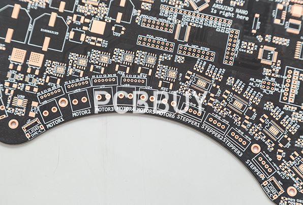
In aerospace and defense applications, multilayer PCBs are used in avionics, communication systems, and radar systems. Their ability to withstand extreme conditions and provide high reliability is essential in these fields.
Case Study: Avionics
Avionics systems require PCBs that can operate reliably in extreme temperatures and vibrations. Multilayer PCBs with 8-12 layers are commonly used, providing the necessary performance and durability.
Industrial Automation
Multilayer PCBs are used in industrial automation for control systems, robotics, and sensors. Their ability to support complex circuits and high-speed data transmission is crucial for these applications.
Case Study: Robotics
Industrial robots require high-performance PCBs to control their movements and functions. Multilayer PCBs with 6-10 layers are used, providing the necessary reliability and performance.
Data and Comparative Analysis
Performance Metrics
To evaluate the performance of multilayer PCBs, several metrics are considered, including signal integrity, thermal management, and mechanical strength. The following table compares these metrics for multilayer, double-layer, and single-layer PCBs:
|
Metric |
Multilayer PCBs |
Double-Layer PCBs |
Single-Layer PCBs |
|
Signal Integrity |
High |
Moderate |
Low |
|
Thermal Management |
Excellent |
Good |
Poor |
|
Mechanical Strength |
High |
Moderate |
Low |
Cost Comparison
The cost comparison between multilayer, double-layer, and single-layer PCBs is presented in the table below:
|
Production Volume |
Multilayer PCBs Cost (USD) |
Double-Layer PCBs Cost (USD) |
Single-Layer PCBs Cost (USD) |
|
1-10 units |
100-200 |
50-100 |
20-50 |
|
11-100 units |
500-1000 |
200-500 |
100-200 |
|
101-1000 units |
2000-5000 |
1000-2000 |
500-1000 |
Environmental Impact
The environmental impact of multilayer PCBs versus double-layer and single-layer PCBs is assessed based on material waste and energy consumption:
|
Aspect |
Multilayer PCBs |
Double-Layer PCBs |
Single-Layer PCBs |
|
Material Waste |
10-15% |
20-25% |
30-35% |
|
Energy Consumption |
15-20 kWh/kg |
10-15 kWh/kg |
5-10 kWh/kg |
What Are Future Prospects and Challenges?
Advancements in Materials
Ongoing research is focused on developing new materials with enhanced properties for multilayer PCBs. High-performance polymers, advanced ceramics, and nanocomposites are among the promising materials being explored.
Integration with Other Technologies
The integration of multilayer PCBs with other advanced technologies, such as artificial intelligence and the Internet of Things (IoT), holds great potential. Smart manufacturing systems can optimize the production process in real-time, further improving efficiency and quality.
Addressing Limitations
Despite their numerous advantages, multilayer PCBs face certain limitations, including higher manufacturing costs and complexity. Continued research and development are essential to overcome these challenges and fully realize the potential of this technology.
Conclusion
Multilayer PCBs represent a transformative approach to electronics manufacturing, offering significant advantages in terms of functionality, signal integrity, reliability, and space efficiency. While there are challenges to be addressed, the ongoing advancements in materials and technology promise a bright future for this innovative method. As the industry continues to evolve, multilayer PCBs are poised to play a pivotal role in shaping the next generation of electronic devices.
Industry Category


