How to Understand HDI PCB Manufacturing?
By:PCBBUY 04/29/2025 16:55
High-Density Interconnector (HDI) Printed Circuit Boards (PCBs) are essential components in modern electronics, enabling the miniaturization of devices while improving performance. With the rapid advancement of technology, HDI PCBs have become increasingly popular in various applications, including smartphones, tablets, and high-performance computing devices. This article provides a comprehensive overview of HDI PCB manufacturing, covering the fundamental principles, processes involved, and the advantages of HDI technology.
What is HDI PCB?
Definition and Characteristics
HDI PCBs are characterized by a higher density of components and interconnections than traditional PCBs. This is achieved through the use of microvias, blind and buried vias, and finer lines and spaces. These features allow for more complex circuitry within a smaller footprint, making HDI PCBs ideal for compact electronic devices.
Types of HDI PCBs
1. Type I: Single-sided HDI PCB with blind and buried vias.
2. Type II: Double-sided HDI PCB with blind and buried vias.
3. Type III: Multilayer HDI PCB featuring multiple layers with microvias.
What Is The HDI PCB Manufacturing Process?
The manufacturing of HDI PCBs involves several key steps:
1. Design and Layout
PCB Design Software
Designing an HDI PCB requires specialized software capable of handling complex layouts. Software such as Altium Designer, Eagle, and KiCAD is commonly used for this purpose.
Design Rule Checks (DRC)
Before proceeding with manufacturing, a thorough Design Rule Check (DRC) is performed to ensure compliance with manufacturing specifications.
2. Material Selection
Substrate Materials
Common substrate materials for HDI PCBs include:
FR-4: A widely used epoxy resin-based material.
Polyimide: Offers excellent thermal stability for high-performance applications.
Ceramic: Used in specialized applications requiring high thermal conductivity.
3. Layer Stacking
The stacking of layers in HDI PCBs is crucial for performance. The arrangement typically follows a specific sequence to optimize signal integrity and minimize crosstalk.
4. Microvia Creation
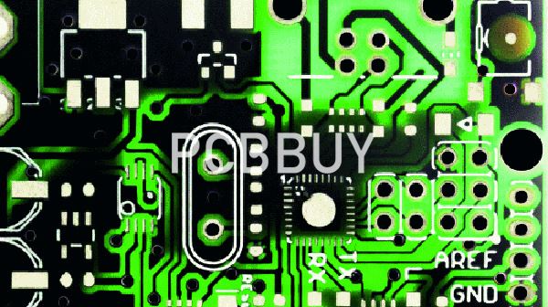
Microvias are created using laser drilling technology, allowing for precise and efficient hole formation. The process involves:
Laser Drilling: High-precision laser systems create microvias, typically with a diameter of less than 150 micrometers.
5. Plating and Etching
Plating Process
Electroless Plating: This chemical process deposits a thin layer of copper onto the substrate. The basic chemical equation for the electroless copper deposition can be represented as:
Cu2+ + 2H2O→Cu + 2H+ + 2OH-
Etching Process
Etching removes unwanted copper from the surface to define the circuitry. Common etching methods include:
Chemical Etching: Utilizing ferric chloride or ammonium persulfate to remove copper.
Laser Etching: Employing lasers for precise etching applications.
6. Lamination
Lamination is the process of bonding different layers of the PCB together. It typically involves:
Prepreg Materials: Pre-impregnated materials are used to bond layers.
Heat and Pressure: Applied to ensure a strong bond between layers.
7. Surface Finishing
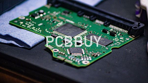
Surface finishing is critical for solderability and protection. Common surface finishes for HDI PCBs include:
HASL (Hot Air Solder Leveling): A traditional finish offering good solderability.
ENIG (Electroless Nickel/Immersion Gold): Provides excellent corrosion resistance and solderability.
OSP (Organic Solderability Preservative): A more environmentally friendly option.
8. Assembly
After manufacturing the PCB, the assembly process involves placing and soldering components onto the board. Techniques used include:
Surface Mount Technology (SMT): Allows for high-density component placement.
Through-Hole Technology: Involves inserting component leads into drilled holes.
9. Testing and Quality Control
Quality control is crucial in HDI PCB manufacturing. Testing methods include:
Automated Optical Inspection (AOI): Checks for visual defects.
X-Ray Inspection: Used for verifying internal connections.
Functional Testing: Ensures the PCB operates as intended.
What Are Advantages of HDI PCBs?
1. Increased Density
HDI PCBs enable a higher component density, allowing for more features within a smaller size. This is particularly beneficial for portable electronics.
2. Improved Performance
The reduced length of traces and the use of microvias enhance signal integrity, leading to improved electrical performance.
3. Cost-Effectiveness
Although the initial manufacturing cost may be higher, the long-term benefits of reduced size, weight, and increased functionality can lead to cost savings.
4. Design Flexibility
HDI technology offers designers greater flexibility in layout and component placement, facilitating innovative designs.
What Are Challenges in HDI PCB Manufacturing?
1. Complexity in Design
The intricate nature of HDI PCB design can lead to increased chances of errors during the design phase.
2. Higher Production Costs
The specialized processes and materials involved in HDI PCB manufacturing can result in higher production costs compared to traditional PCBs.
3. Material Limitations
Finding suitable materials that meet the stringent requirements of HDI technology can be challenging.
Conclusion
HDI PCB manufacturing represents a significant advancement in electronics, offering numerous benefits in terms of performance, density, and design flexibility. As technology continues to evolve, the demand for HDI PCBs will only increase. Understanding the manufacturing process and addressing the associated challenges is essential for companies looking to leverage HDI technology in their products.
References
1. IPC. (2018). IPC-2226: Design Standard for High Density Interconnect PCBs.
2. C. H. Lee, "HDI PCB Design and Fabrication," Journal of PCB Design and Manufacturing, vol. 14, no. 3, pp. 123-135, 2021.
3. H. W. Tsai, "Microvia Technology in PCB Manufacturing," Advanced Materials Research, vol. 1148, pp. 102-108, 2016.
4. B. K. Dutta, "The Impact of HDI PCB Technology on Electronic Product Development," IEEE Transactions on Electronics Packaging Manufacturing, vol. 12, no. 2, pp. 145-155, 2019.
Industry Category


