How to Understand Important Causes of Tombstoning in PCB Assembly?
By:PCBBUY 06/29/2024 15:39

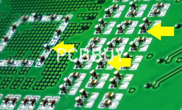
Tombstoning, also known as the Manhattan or Stonehenge effect, is a common defect in Surface Mount Technology (SMT) assembly of printed circuit boards (PCBs). This phenomenon occurs when one end of a passive component, such as a resistor or capacitor, lifts off the PCB while the other end remains soldered, causing the component to stand up vertically like a tombstone. Tombstoning can severely affect the functionality and reliability of electronic assemblies, leading to increased rework and production costs. This article will explore the causes, characteristics, and methods to avoid tombstoning in multilayer PCB assembly.
What Are the Causes of Tombstoning?
Several factors contribute to tombstoning during the reflow soldering process. These factors can be broadly categorized into component-related, PCB-related, solder paste-related, and process-related causes.

Component-Related Causes
1. Component Size and Weight
Small and lightweight components, such as 0201 or 0402 chip resistors and capacitors, are more susceptible to tombstoning due to the imbalance of forces acting on the component during reflow.
2. Component Termination
The type and quality of the component terminations (e.g., silver, tin, or nickel) can affect wetting forces. Poor wetting can cause uneven soldering, leading to tombstoning.
What Are the PCB-Related Causes?
1. Pad Design and Layout
Asymmetrical pad sizes or incorrect pad spacing can cause unequal wetting forces, resulting in tombstoning. IPC-7351 standards provide guidelines for proper pad design to avoid this issue.
2. Solder Mask Design
Solder mask openings that are too large or improperly aligned can cause uneven heating and wetting, contributing to tombstoning.

What Are the Solder Paste-Related Causes?
1. Solder Paste Composition
The alloy composition, particle size, and flux activity in solder paste can influence wetting behavior. High activity fluxes can promote faster wetting on one side of the component, leading to imbalanced forces.
2. Solder Paste Printing
Inconsistent solder paste deposition, such as insufficient or excessive paste on one pad, can create unequal wetting forces, causing tombstoning.
What Are the Process-Related Causes?
1. Reflow Profile
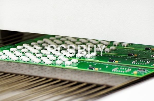
An improperly tuned reflow profile can lead to non-uniform heating. Rapid temperature ramps or uneven heating across the PCB can cause one end of the component to reflow before the other, leading to tombstoning.
2. Conveyor Speed and Oven Zones
Variations in conveyor speed or temperature settings across different reflow oven zones can cause uneven soldering, contributing to tombstoning.
Tombstoning is a complex physical interaction between the component and the solder deposition, and as such, there are multiple process control factors to consider. Primarily, tombstoning arises from three variables:

Torque
Different solder paste chemistries will have different wetting speeds. Ideally, a relatively slow wetting speed is less susceptible to uneven heating during reflow, which is liable to cause different melting rates between the pads. A solder with a longer pasty range slows the wetting speed; alternatively, manufacturers can mix solder alloys to depress the wetting speed, which may incur other production issues. Additionally, thicker or taller chip packages have a greater tendency for tombstoning: as the solder climbs up the pin, its leverage increases. Thin chip packages provide less torque ability to the wetted solder.
Vapor push
At reflow temperatures, some of the solvents in the solder paste will begin to boil off and provide an upward force on the pin. As mentioned above, different solder paste chemistries will contribute more or less to the tombstoning process.
Component float
A paste deposition that is too thick will result in a component floating above the molten solder; an imbalance in pulling forces between the pads often results in tombstoning.
Beyond the paste, the reflow controls will also contribute greatly to eliminating tombstoning in the PCBA. A rapid temperature ramp-up before the reflow zone of the solder leads to a temperature differential between the two pads while compounding the vaporization of the volatile solvents in the solder paste. Therefore, a gradual temperature soak is necessary.
What Are the Characteristics of Tombstoning?
Tombstoning typically manifests as a vertical standing of a passive component on one of its terminations. The following are key characteristics:
1. Vertical Orientation
One end of the component lifts off the PCB while the other remains soldered, creating a vertical or near-vertical orientation.
2. Partial Wetting
The solder fillet is often visible only on one side of the component, indicating partial wetting.
3. Misalignment
The component is usually misaligned with respect to its intended position on the PCB pads.
What Are the Methods to Avoid Tombstoning?
Avoiding tombstoning requires a holistic approach that considers design, materials, and process parameters. Here are several strategies to mitigate the risk:

What Are the Design Guidelines?
1. Pad Design
Ensure symmetrical pad sizes and proper spacing according to IPC-7351 standards to promote uniform wetting forces.
2. Solder Mask Design
Optimize solder mask openings to ensure consistent heating and wetting across the component terminations.
Material Selection
1. Solder Paste
Choose solder paste with appropriate alloy composition, particle size, and flux activity to ensure balanced wetting.
2. Component Selection
Use components with high-quality terminations and consider slightly larger component sizes if feasible to reduce susceptibility to tombstoning.
Process Optimization
1. Reflow Profile
Develop a reflow profile that ensures gradual and uniform heating. Use a soak zone to equilibrate temperatures before reaching the reflow peak.
2. Solder Paste Printing
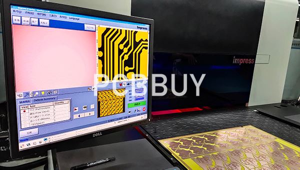
Ensure consistent and accurate solder paste deposition. Use automated optical inspection (AOI) to verify paste placement and volume.
3. Conveyor Speed and Oven Zones
Maintain consistent conveyor speed and optimize oven zone settings to achieve uniform heating across the PCB.
Monitoring and Inspection
1. Automated Optical Inspection (AOI)
Implement AOI to detect tombstoning defects early in the production process.
2. X-ray Inspection
Use X-ray inspection to identify hidden tombstoning defects, particularly in high-density assemblies.

Best DFM Practices to Prevent Tombstoning
There are three main DFM areas to focus on that will help you prevent tombstoning from occurring on your PCB design. By following these recommendations, designers can better avoid tombstoning small passive parts:
Footprint pad size: If the pad sizes for your small passive parts are incorrect, it could affect the thermal mass of the solder joints. A pad with less mass will cause the solder to reflow sooner than larger pads. It is crucial, therefore, to follow industry standards or the manufacturer’s recommended sizes when building the CAD footprint pads.
Footprint construction: Along with building the pads to the correct size, it’s also imperative to ensure the entire footprint for the passive parts is correct. Pads also require the correct pitch (pad spacing) and identical size pads for both part pins. Again, the key is to follow industry standards and the manufacturer’s recommendations when building footprints.
Trace routing and power planes: Even with a perfectly sized and balanced CAD footprint, there could still be a risk of differing thermal mass between the pads if the routing is unequal. Connecting one pad with a thin trace while connecting the other pad with a thick trace will create an imbalance in the thermal mass of the two pads. The additional metal will act as a heat sink, causing the solder paste on that pad to melt slower than the other. Embedding a pad within a power plane is even worse, as the larger metal area will pull more heat with it. Be careful to balance the routing between the two pads as much as possible, and use thermal ties when connecting a pad directly to a metal plane.
Conclusion
Tombstoning is a prevalent defect in PCB assembly that can significantly impact the reliability and performance of electronic devices. By understanding the causes and characteristics of tombstoning, manufacturers can implement design, material, and process optimizations to mitigate this issue. Adopting a comprehensive approach that includes proper pad design, material selection, reflow profile optimization, and thorough inspection can help minimize the occurrence of tombstoning and improve overall assembly quality.
References
1. IPC-7351: Generic Requirements for Surface Mount Design and Land Pattern Standard.
2. N. Ahmad, "Investigation of Tombstoning Defect in Surface Mount Assembly," Journal of Electronics Manufacturing, vol. 9, no. 3, pp. 185-195, 2019.
3. J. H. Lau, "Thermal Stress Analysis of Electronic Packages," Electronic Components and Technology Conference (ECTC), 2020.
4. K. W. Song and C. T. Chen, "The Impact of Solder Paste Composition on Tombstoning in SMT Assembly," IEEE Transactions on Electronics Packaging Manufacturing, vol. 32, no. 2, pp. 78-85, 2020.
5. R. Prasad, "Surface Mount Technology: Principles and Practice," Springer, 2021.
Industry Category


