How to Understand PCB Pattern Transfer Process?
By:PCBBUY 12/20/2024 14:10
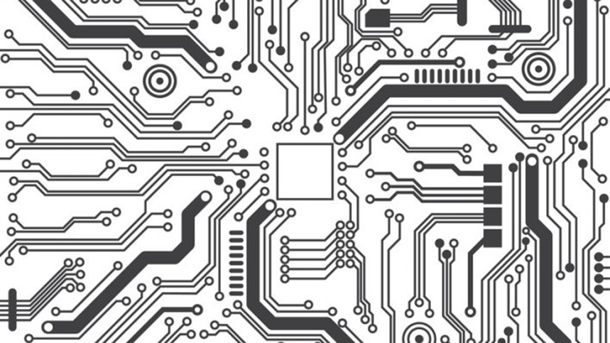
Printed Circuit Boards (PCBs) are the backbone of modern electronic devices, providing the necessary electrical connections between components. One critical stage in PCB fabrication is the pattern transfer process, which ensures that the designed circuitry is accurately imprinted onto the board. This article delves into the principles, methodologies, and scientific basis of PCB pattern transfer, supported by chemical equations, data, and comparisons.
1. Introduction
Printed Circuit Boards (PCBs) play a crucial role in the functionality of electronic devices, providing mechanical support and electrical connectivity. The pattern transfer process in PCB manufacturing is essential for creating the conductive paths that interconnect electronic components. This article explores the intricacies of PCB pattern transfer, detailing various methods, materials, chemical processes, and the future of this technology.
2. Overview of PCB Fabrication
PCB fabrication involves multiple stages, from design and material selection to pattern transfer and final assembly. The primary steps include:
1. Design and Layout: Using Computer-Aided Design (CAD) software to create the circuit layout.
2. Substrate Preparation: Selecting and preparing the board material, typically fiberglass-reinforced epoxy resin (FR-4).
3. Pattern Transfer: Transferring the circuit pattern onto the substrate.
4. Etching: Removing unwanted copper to create the desired circuitry.
5. Drilling and Plating: Creating holes for component leads and vias, followed by plating to ensure conductivity.
6. Solder Mask and Silkscreen Application: Adding protective layers and component labels.
7. Component Assembly and Testing: Placing and soldering components, followed by testing for functionality.
3. Principles of Pattern Transfer
The pattern transfer process involves transferring the designed circuitry from a digital layout to the physical PCB substrate. The accuracy and precision of this process are crucial for the functionality of the final product. The two primary techniques for pattern transfer are additive and subtractive processes.
Additive Process
In the additive process, conductive material is deposited only where needed. This method includes techniques like electroless plating and inkjet printing. However, the subtractive process is more commonly used in PCB fabrication.
Subtractive Process
In the subtractive process, a thin layer of copper covers the entire surface of the substrate, and the unwanted copper is removed through etching. The desired circuit pattern is protected by a mask during the etching process.
4. Methods of Pattern Transfer
4.1 Photolithography
Photolithography is the most widely used method for pattern transfer in PCB manufacturing. This process uses light to transfer a geometric pattern from a photomask to a light-sensitive chemical (photoresist) on the PCB substrate.
Process Steps
1. Coating: Applying a layer of photoresist on the copper-clad substrate.
2. Exposure: Exposing the photoresist to ultraviolet (UV) light through a photomask.
3. Development: Developing the exposed photoresist to reveal the circuit pattern.
4. Etching: Etching away the exposed copper.
5. Stripping: Removing the remaining photoresist.
Chemical Equations
The development of photoresist involves chemical reactions, such as:
Photoresist (PR) + UV Light→Exposed PR
For positive photoresists:
Exposed PR + Developer→Soluble PR
For negative photoresists:
Exposed PR+Developer} →Insoluble PR
Advantages and Disadvantages
|
Advantages |
Disadvantages |
|
High precision and resolution |
Expensive equipment |
|
Suitable for mass production |
Sensitive to environmental conditions |
4.2 Direct Imaging
Direct imaging (DI) is a modern technique that eliminates the need for photomasks by using a computer-controlled light source to directly expose the photoresist.
Process Steps
1. Coating: Applying photoresist to the substrate.
2. Direct Imaging: Using laser or LED light to expose the photoresist according to the digital design.
3. Development: Developing the exposed photoresist.
4. Etching: Removing the unwanted copper.
Advantages and Disadvantages
|
Advantages |
Disadvantages |
|
Eliminates photomask cost and alignment issues |
High initial setup cost |
|
Faster turnaround time |
Limited to specific photoresist types |
4.3 Screen Printing
Screen printing is a simpler and cost-effective method for pattern transfer, typically used for less complex PCB designs.
Process Steps
1. Screen Preparation: Creating a screen with the desired pattern.
2. Ink Application: Applying conductive or etch-resistant ink through the screen onto the substrate.
3. Curing: Curing the ink to harden it.
4. Etching: Removing the unwanted copper.
Advantages and Disadvantages
|
Advantages |
Disadvantages |
|
Low cost |
Lower resolution |
|
Suitable for prototypes and small batches |
Not suitable for fine-pitch components |
5. Materials Used in Pattern Transfer
Photoresists
Photoresists are light-sensitive materials used to create patterns on the PCB. They can be classified into positive and negative photoresists.
Positive Photoresists: These become soluble when exposed to light.
Negative Photoresists: These become insoluble when exposed to light.
Etching Solutions
Etching solutions are chemicals used to remove unwanted copper from the PCB substrate. Common etching solutions include:
Ferric Chloride (FeCl3):
Cu + 2 FeCl3→CuCl2 + 2FeCl2
Ammonium Persulfate ((NH4)2S2O8):
Cu + 2 (NH4) 2S}2O8 →CuSO4 + 2NH4HSO4
Substrate Materials
Common substrate materials include:
FR-4: A glass-reinforced epoxy laminate.
CEM-1 and CEM-3: Composite epoxy materials.
Polyimide: Used for flexible PCBs.
6. Chemical Processes Involved
6.1 Photoresist Chemistry
The chemistry of photoresists involves the interaction between light and the photoactive compounds in the resist. This interaction changes the solubility of the resist in a developer solution.
6.2 Etching Solutions
Etching solutions chemically react with the copper layer, dissolving the unprotected areas. The choice of etching solution depends on the specific requirements of the PCB design.
Comparison of Etching Solutions
|
Etching Solution |
Advantages |
Disadvantages |
|
Ferric Chloride |
Cost-effective, widely used |
Generates hazardous waste |
|
Ammonium Persulfate |
Cleaner etch, less undercutting |
More expensive |
7. Comparison of Pattern Transfer Techniques
|
Technique |
Resolution |
Cost |
Production Volume |
Turnaround Time |
|
Photolithography |
High |
High |
High |
Moderate |
|
Direct Imaging |
High |
High |
Low to moderate |
Fast |
|
Screen Printing |
Low to moderate |
Low |
Low |
Fast |
8. Challenges and Solutions in Pattern Transfer
Challenges
1. Alignment Issues: Ensuring precise alignment between layers.
2. Resolution Limits: Achieving fine features in complex designs.
3. Environmental Sensitivity: Controlling temperature, humidity, and light exposure.
Solutions
1. Advanced Equipment: Using high-precision alignment tools and automated systems.
2. Improved Materials: Developing higher resolution photoresists and etching solutions.
3. Controlled Environment: Implementing cleanroom conditions for sensitive processes.
9. Future Trends in PCB Pattern Transfer
1. Laser Direct Imaging (LDI): Increasing adoption for higher precision and faster turnaround.
2. Nanoimprint Lithography: Potential for even finer resolution and lower costs.
3. Environmental Sustainability: Development of eco-friendly materials and processes.
Conclusion
The pattern transfer process is a critical step in PCB manufacturing, with various methods available to suit different needs and applications. Understanding the principles, materials, and chemical processes involved is essential for producing high-quality PCBs. Continuous advancements in technology and materials are driving the evolution of this field, promising higher precision, efficiency, and sustainability.
References
1. R. C. Dorf, "The Electrical Engineering Handbook," CRC Press, 2000.
2. M. S. Makel, "Printed Circuits Handbook," McGraw-Hill, 2016.
3. T. K. Sarkar, "Handbook of Antennas in Wireless Communications," CRC Press, 2001.
4. D. Lu, "Materials for Advanced Packaging," Springer, 2008.
5. M. Pecht, "Handbook of Electronic Package Design," CRC Press, 1991.
6. H. Nakajima, "Chemical and Biological Sensors for Environmental Monitoring," Springer, 2008.
Industry Category

