How to Understand PCB and the Cutting-edge Technology of 5G Communication?
By:PCBBUY 06/25/2024 17:22
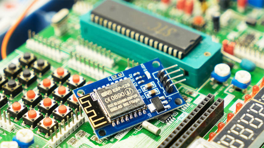
In recent years, consumer mobile communication terminal products represented by mobile phones and tablet computers have experienced rapid development, among which the development of smart phones basically represents the relevant electronic components such as IC(Integrated Circuit) in the past 10 years. PCB(Printed Circuit Board) and the development of other passive electronic devices. The development of mobile communication terminal products requires the application of smaller PCB areas, more refined lines, chip and passive device functions are constantly enhanced, while having high reliability performance. At the same time, the comprehensive screen, the high frequency of signal transmission and the continuous improvement of battery performance are also the development needs of communication terminal products.
As the "mother of electronic products", PCB is an important connection carrier for various functional components and passive devices, which affects the important performance of communication terminal products. Around 2003, the PCB size is generally about 130mm×50mm, and its size is comparable to the size of the mobile phone. At that time, the mobile phone suppliers represented by Apple and Samsung, the line width and line distance of PCB could be 100μm/100μm, and the production of blind holes was realized, that is, the HDI board with 1+n+1 structure. After 10 years of development, entertainment, web browsing, life, transportation and other aspects of intelligent terminal products "show their skills", which has promoted the function and performance of intelligent terminals. However, the PCB did not increase the size, but reduced to about 20cm2 (iPhone 85mm×20mm), thanks to the development of HDI technology. PCB line width line distance 40μm/40μm, blind hole φ45μm or so, and the use of any layer interconnection method makes the density of intelligent terminal PCB increased by more than 6 times.
PCB miniaturization and multi-function is the eternal pursuit of intelligent terminal products. In the second half of 2017, the release of iPhone X products led the communication terminal products into a new era. The application of technologies such as Chip on flex (COF), SLP(Substrate Like PCB), 2.5D and WLP(Wafer Level Packaging) has led to the realization of a new generation of full-screen, 3D face recognition and long-standby intelligent terminals. This paper will analyze and introduce the above several key PCB manufacturing technologies, and specifically elaborate the development of PCB technology for next-generation communication terminal products.
Mobile Communication Terminal Application PCB Cutting-edge Technology
COF(Chip On Film) technology
In the communication terminal represented by smart phones, FPC(Flexible Printed Circuit) has been used on a large scale. The number of FPC used in a single terminal product is generally 10 to 15 pieces. Among them, FPC for display signal transmission and control is essential. The work of the display depends on the control of the corresponding IC. The traditional method is to use COG(Chip on Glass) packaging. Since FPC is a flexible substrate, in order to realize the chip packaging and fixing, COG must rely on the display glass carrier to package the IC and FPC, as shown in Figure 1a below. Smartphones packaged in this way generally have a "chin" picture at the bottom of the phone.
In order to completely realize the full screen of smart phones, the packaging method of COG must be abandoned, and COF is a very good choice. As shown in FIG. 1b, COF is to mount bare display ics directly on FPC, and use Anisotropic Conductive Film (ACF) to realize electrical connection and fixation between IC and FPC.
In COF technology, ACF packaging and FPC production become the key processes. The process flow chart of FPC production is shown in Figure 2 below. The production of FPC in COF is not significantly different from that of conventional products, but it has more stringent requirements in line fineness and dimensional error. At present, the IC welding foot spacing is usually less than 50μm, which is mainly 20~30μm. In addition, the line size error should be ≤15%. Therefore, in terms of material selection and process control, COF production with FPC requirements are more stringent. In the process of processing, the size control, the error of the line graphics transfer, must be effectively controlled.
In order to reduce the space that the chip occupies on the surface of the FPC, the display driver chip is usually welded with the FPC via the bare chip ACF, rather than the traditional SN-based solder. ACF is a kind of anisotropic conductive film. Before welding, ACF resin is evenly dispersed in a large number of nano-metal particles (usually mainly Ag nanoparticles), and the nanoparticles are insulated between them, so ACF is not conductive before welding. After welding, the IC bare chip and PFC welding foot are welded together by heating and pressurizing. At this time, during the pressurization process, the IC chip's welding foot and the FPC welding foot are close, and the uniformly dispersed nano metal silver becomes the electrical connection point between the connection welding, which can realize the current carrying or signal transmission picture. However, in the X and Y directions, due to the insulation between the conductive film nano-metals, the conductive film is not conductive, so that the anisotropic electrical transmission of the conductive film is realized. ACF is the key material, the current market mainstream ACF material provided by SONY and Hitachi.

SLP(Substrate Like PCB) technology
SLP is a new generation of technology for the further development of miniaturization, refinement and thinness of HDI. Because it has the same high wiring density as the package substrate, it is also known as the carrier board. Generally, the line of SLP printed circuit board products is ≤40μm, and the aperture is ≤ picture. In 2017, SLP technology was applied to the new generation of iPhone 8 and iPhone X mobile phones, and its line width/line distance reached 30μm/30μm, and the blind hole picture represents the highest technical level of the printed circuit board of the communication terminal.
In SLP technology, the production of hyperfine circuits becomes a crucial Process, the core of which is the use of SAP(Semi-Additive Process) or mSAP(modified Semi-Additive Process) method to ensure the feasibility of SLP, as shown in Figure 4 below. In the flow chart, considering that the late ultra-thin copper foil needs to be browned (usually requires the etching of copper about 1μm thick) for laser drilling, the thickness of the ultra-thin copper foil is usually between 1 and 3μm, and has good uniformity. After that, the ultra-thin copper foil is browned, laser drilling and other processes to form blind holes on the substrate. Electroless copper plating and electroplating hole filling fill the blind hole with copper to achieve electrical connection between layers. The circuit pattern is transferred to the dry film by laser direct imaging (LDI) technology, and then the fine circuit pattern is obtained by electroplating thickening line, removing film and differential etching.
mSAP is short for the modified semi-addition method, and its modification is intended to reduce the cost of the conventional use of expensive thin copper foil (thin copper foil illustrated in Figure 4). Therefore, in the mSAP process, the preparation of thin copper foil is very important. The easiest way to obtain ultra-thin copper foil is to reduce it with a low-cost 9μm or 12μm thick copper foil. In this process, the standard thickness copper foil is laminated with a semi-cured sheet and then thinned with a thinning solution. Due to the "pool effect", the biggest problem of this method is to obtain ultra-thin copper foil with high uniformity. Current etching fluids for printed circuit boards can be used as thinning solutions. However, studies have shown that picture etching fluid can obtain better uniform pictures of thin copper foil.
The thinning of standard copper foil is not the most ideal way to obtain ultra-thin copper foil. It is more uniform to make ultra-thin copper foil on the insulating substrate by sputtering or electroless copper plating. However, the biggest problem with this method is the binding force between the added layer of copper foil and the insulating substrate. Ti and resin have a good effect, therefore, by sputtering Ti/Cu to obtain 1~3μm thick ultra-thin copper foil can meet the requirements of fine line bonding force. However, the cost of sputtering Ti/Cu is high and the production efficiency is low, so it is difficult to apply in the field of printed circuit boards on a large scale. In addition, in the differential etching process, the etching solution of Cu can not etch Ti, so it is necessary to add additional steps to etch Ti layer.
It is a low-cost method to make ultra-thin copper foil on the substrate by electroless copper plating. However, the problem to be solved is the binding force between the electroless copper plating layer and the insulating substrate. The combination between traditional electroless copper plating and resin is mainly achieved by coarsening anchorage. The binding force is improved by increasing the roughness of the resin. However, the ability of anchoring method to improve the binding force is limited, and it is not suitable for the production of fine lines. High binding force under low roughness is the application requirement of electroless copper plating to obtain ultra-thin copper foil. The chemical bonding between copper and resin is an important solution.
Whether mSAP or SAP technology, differential etching is an essential process. Differential etching is the process of removing unnecessary ultra-thin copper foils after electroplating addition of fine lines. Because the fine lines of electroboardd thickened are not protected by dry film fine, the thickened fine lines are etched while the ultra-thin copper foil is removed in the differential etching process, and the etching speed of the thickened fine lines is faster than that of the ultra-thin copper foil. The traditional etching solution or etching method will have a great influence on the size of the thickened fine line, such as thinning and narrowing of the line, and the reduction of the etching factor. Figure 7 shows the fine line (line width/line distance of 45μm/45μm) obtained by differential etching using traditional etching methods.
The fine line after electroplating presents a square shape, but as shown in Figure 7, after differential etching, both sides of the surface of the line are particularly easy to be etched off, thus presenting a trapezoidal structure. In Figure 7, the fine line has an etching factor of about 4. Therefore, the ideal etching method is to be able to protect both sides of the fine line surface with an effective protective agent to obtain a high etching factor profile. Benzimidazole organics are good adsorbents for copper, which can be easily adsorbed on copper surface to prevent etching by etching solution. Based on the tip effect, the amount of protective agent is the most at both ends of the surface of the fine line, while the adsorption amount on the ultra-thin copper foil surface and the side of the line is relatively small. In the etching process, the two ends of the surface of the fine line are effectively protected, so that the square shape of the fine line remains the original appearance after differential etching. Figure 8 shows the etching mechanism of the method and the profile of the obtained fine line (line width/line distance: 30μm/30μm).
In addition, in SLP laser drilling, conventional brown-modified copper foil is required to achieve copper foil absorption of image laser, and its Browning roughness is 2~3μm(Rz), while the thickness of thin copper foil is only 1~3μm. Therefore, low roughness (≤1μm) Browning technology must be used. In addition, coating the surface of the copper foil with an auxiliary light-absorbing material about 100nm thick can help the picture laser to break down the thin copper foil. UV laser can directly break down copper foil, so using UV laser to make blind holes is also an important method, but its difficulty lies in the depth control of laser drilling.
In order to improve the adhesion between the fine line and the semi-cured sheet, the fine line is often browned before laminating. The roughness of 2~3μm makes the size of the fine line change obviously, which deviates from the design requirements of the line. Unlike the laser Browning in the picture, the size of the bonding force depends on the roughness of the Browning. The greater the roughness, the better the binding force. Therefore, non-etched surface enhancement technology has become an important solution to this problem. Figure 9 shows the fine lines obtained by the two methods. In the non-etched surface treatment technology, the isopotential points on the surface of copper foil can be modified to reduce the isopotential points on the surface, so that better bonding force can be obtained without roughening the surface.
WLP(Wafer Level Packaging)Fan Out technology
WLP, that is, wafer level packaging, is a new development of IC packaging technology in recent years. Conventional IC packaging is done by welding the wafer to the IC packaging substrate, and then welding the IC substrate to the ordinary PCB picture. The WLP package is based on IC wafers, using PCB manufacturing techniques, such as the production of lines and holes, to form a structure similar to the IC package substrate on the wafer. The IC of the structure can be directly installed on the ordinary PCB board after plastic sealing. WLP has been used since the Apple A10, which greatly saves the surface area of the motherboard.
Fan In WLP can only limit its wiring and solder pin to the chip size, while Fan Out WLP can be extended beyond the chip size and even achieve the chip stacking. Therefore, Fan Out WLP can achieve higher density chip packaging and become the mainstream technology of WLP in the future. Compared with conventional packaging technologies, Fan Out WLP has the following advantages:
(1) Significantly increase the I/O interface density;
(2) It is beneficial to realize the extension of SiP(System in Packaging) technology;
(3) Better electrical and thermal performance;
(4) Higher reliable performance;
(5) The package line is more fine (currently 10μm/10μm).
In the future, it is feasible to achieve fine lines of 2μm/2μm by Fan Out packaging directly on the wafer.
2.5D platform technology
2.5D platform technology is a concept proposed by AT&S for the stepped surface of printed circuit boards. The use of 2.5D platform technology can realize multi-dimensional installation of printed circuit boards, reduce the thickness of IC and device installation area, and is conducive to anti-electromagnetic interference picture. In some cases, in order to maintain the high consistency of the welded chip and the surface of the printed circuit board, the height of the chip is reduced by digging a trench in the printed circuit board, so that the chip is installed in the trench. In addition, 2.5D technology is also required for stiff-flex bonding boards. The iPhone X motherboard released by Apple in 2017 uses two motherboards welded together, and the motherboard uses 2.5D platform technology. In 2.5D platform technology, the key technology of its production is the production of ladder.
Mobile Communication Terminal Application PCB Next Generation Technology
In recent years, consumers have increasingly high requirements for the application of mobile communication terminals represented by smart phones. Among them, high screen occupancy, long battery life, and strong functions have become typical application requirements. For a long time, in order to improve the battery life of mobile communication terminals, the battery occupies more and more space in the mobile phone, which leads to the gradual reduction of the area and volume occupied by the PCB. The design of the iPhone X motherboard is typical of making room for batteries, and this trend will continue. Therefore, the development of printed circuit boards with smaller areas or volumes has become an important demand for the next generation of mobile communication terminals.
Embedded Component Packaging (ECP) technology
Taking the iPhone X as an example, passive devices such as resistors, capacitors, and inductors occupy about 60% of the printed circuit board. The reduction of PCB size in the next generation of mobile communication terminals and the reduction of the number of passive devices mounted on the PCB surface is imperative. Therefore, the ECP technology of embedding passive devices into the PCB has become an important solution. When embedded in the PCB, the following advantages can be achieved:
(1) The printed circuit size can be smaller;
(2) The protection of solder joints improves the reliability of passive device installation;
(3) Passive/active devices can be embedded and reduced
For now, both approaches have their pros and cons. The advantages of embedded discrete device technology are that the process flow is fixed, it is easy to achieve standardized production, and because the functional value of discrete devices is stable, the electrical transmission performance is guaranteed. In addition, as discrete device sizes have become smaller in recent years, PCB sizes can be lower. However, the disadvantage is that the embedded discrete devices are easy to cause the Z-direction size of the PCB to be large, and the reliability of the solder joint is also a problem. The process flow of embedded integrated devices has good compatibility with PCB and is easy to be industrialized. Because the device formed directly from the material realizes the planarization, the size change in the Z direction is small. In addition, the material forming of the device ensures the reliability of direct welding with the line. However, the disadvantage is that the core material is monopolized, the price is expensive, and the embedding process of different devices is different, which is not conducive to standardized production, and the stability of the functional value of the device is poor. Considering the stability of PCB electrical transmission, ECP technology applied to mobile communication terminals will adopt the method of embedding discrete devices.
Rigid -flex bonding board technique
Rigid flexible bonding board was proposed as early as 2000, and gradually used in mobile communication terminals. As a product that can realize 3D installation, rigid flexible bonding boards will be widely used in the next generation of mobile communication terminal PCBS. Take the iPhone X motherboard as an example, its two PCBS have a total of 4 surfaces, and its connectors and solder joints occupy at least one surface, that is, 25% of the surface area. If the connectors and solder joints are transferred to the side of the PCB, that is, using stiff-flex bonding board technology, the PCB area can be further reduced.
By using rigid flexible bonded board technology, two or even multiple boards can be stacked by 180° bending of the flexible board, and the solder joint is transferred from the surface to the side, saving the solder joint area; Flexible board is used to connect the hard board, which has higher reliability; Easy assembly and disassembly; The flexible board of other functional modules can be integrated to reduce the use of the number of connectors.
In recent years, the mobile communication terminal is the most competitive electronic product in the market, and its product components have also become the technical "wind vane" in various fields. As an important electronic component of mobile communication terminals, PCB represents the most cutting-edge technologies in the field such as COF, SLP, WLP Fan Out and 2.5D platform technology. ECP and rigid bonded board technology will further realize the miniaturization of PCB from the aspects of device installation and PCB space layout, and will also become an important technology for the next generation of PCB.
Reference
He Wei, PCB Basic Electrical Information Science and Technology, China Machine Press,432-437
Industry Category


