Understanding PCB Microvia Technology
By:PCBBUY 11/25/2024 17:24

PCB Microvia Technology is revolutionizing the electronics industry, enabling the development of compact, high-performance devices. As the demand for miniaturization and enhanced functionality grows, microvias have become a critical component in High-Density Interconnect (HDI) PCB designs. This in-depth guide explores the structure, fabrication process, benefits, challenges, and future trends of PCB microvia technology, helping engineers and manufacturers stay ahead in the rapidly evolving electronics landscape.
What Is PCB Microvia Technology?
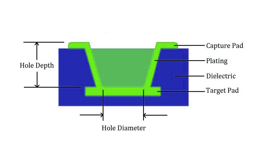
PCB microvias are miniature vias—typically with a diameter of less than 150 µm—used to establish electrical connections between layers in HDI printed circuit boards. Unlike traditional through-hole vias, microvias support more compact and reliable designs by minimizing space consumption and reducing signal path lengths. This innovation is fundamental to modern electronics, especially in applications where space, weight, and signal integrity are critical.

Types of Microvias in PCB Microvia Technology
Understanding the different configurations of microvias is essential for optimizing HDI PCB designs. The primary classifications include:
-
Blind Microvias: Connect outer layers to internal layers without going through the entire board.
-
Buried Microvias: Link only internal layers, remaining hidden from external view.
-
Stacked Microvias: Vertically aligned and filled vias, enabling interconnection between multiple layers.
-
Staggered Microvias: Misaligned microvias offering layer-to-layer connectivity without overlapping.
These structures enable flexible routing options in complex, multilayer HDI PCBs.

Manufacturing Process of PCB Microvia Technology
The PCB microvia fabrication process involves several highly controlled steps to ensure precision and reliability:
1. Laser Drilling for PCB Microvias
Laser drilling is the most common method for forming microvias due to its ability to produce precise, clean holes. Two types of lasers are typically used:
-
CO₂ Lasers: Suitable for drilling through dielectric materials.
-
UV Lasers: Ideal for achieving finer, cleaner holes with less thermal stress.
2. Copper Plating in Microvia Structures
Once drilled, microvias are plated with copper to establish conductivity:
-
Electroless Copper Plating: Deposits an initial conductive layer inside the via.
Chemical Reaction:
Cu²⁺ + 2HCHO + 4OH⁻ → Cu + H₂ + 2HCOO⁻ + 2H₂O -
Electrolytic Plating: Enhances copper thickness for improved mechanical strength.
3. Microvia Filling
Filled microvias, typically using copper or conductive epoxy, provide structural integrity and enable via stacking in HDI PCB designs.
4. Surface Finishing
Final treatments—such as the application of solder masks and ENIG (Electroless Nickel Immersion Gold)—enhance durability, solderability, and corrosion resistance.

Benefits of PCB Microvia Technology
The advantages of adopting microvia technology in PCB manufacturing include:
| Feature | Microvias | Traditional Vias |
|---|---|---|
| Via Diameter | <150 µm | >250 µm |
| Penetration Depth | Partial | Full through-hole |
| Fabrication Method | Laser Drilling | Mechanical Drilling |
| Signal Integrity | Excellent | Moderate |
| Cost | Higher | Lower |
Key Advantages:
-
Device Miniaturization: Supports compact, lightweight electronics.
-
Improved Signal Integrity: Reduces delay, interference, and crosstalk.
-
Enhanced Thermal Management: Aids in heat dissipation for high-power systems.
-
High Routing Density: Allows for more complex and multilayer PCB layouts.

Applications of PCB Microvia Technology
PCB microvia technology is utilized in various advanced electronics sectors, including:
-
Consumer Electronics: Smartphones, smartwatches, and AR/VR devices.
-
Automotive Systems: ADAS, electric vehicle control units, and infotainment.
-
Medical Electronics: Miniaturized diagnostic and wearable medical tools.
-
Telecommunication Equipment: 5G infrastructure and high-speed modems.
-
Aerospace and Defense: Space-constrained, high-reliability applications.

Challenges in Implementing PCB Microvia Technology
Despite its significant benefits, PCB microvia technology presents several challenges:
-
Higher Manufacturing Costs: Due to advanced drilling and plating processes.
-
Thermal and Mechanical Stress: Especially in stacked microvia configurations.
-
Inspection Complexity: Requires high-resolution X-ray or AOI (Automated Optical Inspection) systems to detect voids or delamination.
Future Trends in PCB Microvia Technology
As technology continues to advance, PCB microvia technology is evolving to meet new demands:
1. Ultra-Fine Microvias (<100 µm)
Emerging UV laser systems and thinner copper foils allow for even smaller microvia structures, ideal for ultra-dense and miniaturized PCB applications.
2. Improved Stacked Microvia Reliability
Enhanced filling techniques, such as copper electroplating and laser via alignment, are increasing the durability of stacked microvias in HDI boards.
3. Advanced Material Development
-
Low Dk/low Df Dielectrics: For improved signal performance at high frequencies.
-
Thermal Epoxies: To handle power-dense applications without degradation.
4. Integration with AI and Automation
-
Smart Inspection Tools: AI-based X-ray systems can detect sub-micron defects.
-
Process Control Optimization: Machine learning aids in improving yield and consistency.
5. Cost Efficiency Innovations
-
Batch Laser Drilling: Reduces production time and cost per unit.
-
Material Recycling: Lowers environmental impact and raw material expenses.
6. Environmentally Friendly Processes
-
Reduced Chemical Waste: Eco-friendly plating and cleaning methods are being implemented.
-
Water-Based Cleaners: Replacing solvent-heavy alternatives in surface prep.
7. Expansion into Emerging Technologies
-
Wearables and Flexible Electronics: Flexible microvias suit non-rigid substrates.
-
Autonomous Driving Systems: High-density boards enable advanced AI processing.
-
Quantum Computing: Microvias facilitate ultrafine connections in quantum logic circuits.
Conclusion
PCB microvia technology is not just a trend—it's a necessity for modern electronic design. It empowers innovation by enabling smaller, more reliable, and higher-performance devices. From smartphones to aerospace systems, microvias are the invisible backbone that drives functionality and efficiency. As manufacturing techniques and materials continue to evolve, the future of PCB microvia technology looks more promising than ever.
✅ Optimize Your PCB Designs with Advanced Microvia Technology
Partner with trusted manufacturers to harness the full potential of PCB microvia technology. Whether you're developing IoT devices, automotive systems, or medical electronics, microvias provide the performance edge your PCB products need.
Industry Category


