How to Use AI PCB Design for Layout Manufacturing Process?
By:PCBBUY 10/13/2023 17:07

The process of PCB design involves multiple steps of optimization. Rarely does any design stage avoid a revision to better suit functionality or performance. The majority of these optimizations are backward-looking; that is, design or production needs to progress to a point where evaluation can be made on prior work. Whether by simulation or a more tangible method, a feedback loop is established where operators engineer for the most desirable traits and seek the best practices to bring them about. This design for manufacturing methodology can be made self-selecting with AI encoding that mimics evolutionary niches.
For design, placement can proceed where non constrained components (not bound to a particular x,y-coordinate) can be automated. By setting criteria, computers can evaluate these placements and assign a rating based on how closely they adhere to their stated goal. Candidates that show excellent scores can be maintained, while those showing promise will be subject to some change in the hopes of inducing greater performance. Though AI solutions for placement remain computationally intensive and therefore prohibitive for most, the emerging field shows promise for machine-assisted layout.
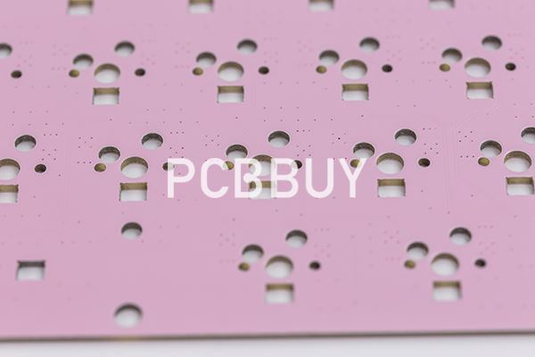
Manufacturing cannot be as receptive to on-the-fly adjustments as the design stage due to various inputs like cost, time, and equipment availability. Rather, AI tools can inspect and refine fabrication and assembly processes to catch defects at the earliest possible production stage for decreased scrap/rework and improved yield. The most prominent field is computer vision, which aims to improve traditional visual inspection modes in speed and accuracy. AI in optical inspection relies on convolution neural networks, which, through various mathematics and organizational algorithms, can break down an image into smaller pieces that only activate filters within a small area. These small receptive fields of these filters are designed on the operating principle of biological vision acquisition.
How Computer Vision Can Fight Counterfeits?
Computer vision is strongly associated with defect detection, but it also can serve an important role in discovering counterfeit components. With supply chains still reeling from pandemic-related shutdowns and underutilized production lines, the demand for components remains a bottleneck, sending demand sky-high. To make matters worse, forgeries have begun to enter the market acceleratedly to take advantage of the component supply-demand gap. These adulterated parts pose numerous detriments, such as:

Reliability: Malicious component insertion could allow attackers to bypass security systems and act as a hardware Trojan horse; in IoT-enabled systems, this could lead to a breach of confidential user data. Mislabeled or otherwise deceiving parts can disrupt the functionality or lead to early component failure (potentially catastrophic), either of which endangers the long-term dependability of the board. The inability to catch falsified parts for high-reliability electronics can pose potentially lethal results.
Production scheduling: Even counterfeit devices successfully detected in-circuit still require replacement and desoldering/rework to restore the board to its earlier state. Remediation on a large scale may significantly hinder manufacturing lines and increase time-to-market.
Environmental safety: Reused or recycled components may not adhere to current regulations such as RoHS and could incur additional costs due to enforcement, recall, or disposal.
Training systems on components face more challenges than simple defect identification. While most defects have clear identifying markers that separate them from a compliant feature, the sheer swath of component packages available can quickly overwhelm a supervised machine-learning architecture. To further complicate matters, the recency of computer vision applications to counterfeit detection means there are no classification standards for devices that straddle different circuit functions. Miniaturization also can compound imaging efforts, and board features may be mistakenly analyzed as a component. In short, visually recognizing components evolves from year to year and between manufacturers and boards.

Though only now in its infancy, industry and academia have engaged in research that looks to apply computer vision to reverse-engineer a bill of materials (BoM) from a particular board and compare it against the provided BoM while searching for discrepancies. Much like “known good” comparisons common in manufacturing tests, this theoretical BoM would serve as the standard by which to judge any experimental board. Though trepidation may exist around the technology’s use to bypass IP, the ability to leverage computer vision to further quality assurance likely outweighs any drawbacks.
Industry Category


