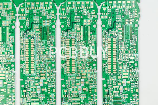
How to Use PCB Cloning to Reduce the Shutdown in Manufacturing?
By:PCBBUY 09/28/2023 16:49

To address the elephant in the room, reverse engineering is not inherently immoral or an attempt to subvert the works of rights holders. Reverse engineering is an information-gathering practice. While it can be employed for nefarious purposes, a design team may want to produce a PCB clone for numerous valid reasons. Some of those reasons are as follows:
Lost, damaged, or inaccessible manufacturing data: A loss of backup files or corruption can significantly slow down the board revision process. Designers may encounter delays or difficulties retrieving data sent to manufacturers, or internal access to data may be compromised or lost. Physical hardware can be damaged, and service to digital backups can be interrupted, but a manufactured board will always function as a literal physical copy of the board design.

Legacy hardware: All printed circuit hardware eventually reaches a period of obsolescence, whether planned by the manufacturer to shepherd users over to a new device iteration or as a result of defunct technology or OEMs. In the latter case, it is a two-tiered problem of availability. That means as new technology replaces old, replacements become harder to source.
Interoperability: Devices need to communicate and interface, and understanding the mechanisms to do so, or how to best optimize these methods for improved performance between devices, can be an acceptable use for reverse engineering.
Standard PCB development cycles begin with a schematic that serves as a controlling document, but when these files are not available, designers must either dedicate significant time to recreating the schematic based only on the superficial knowledge of the product or piece it together from the design information contained within the board itself.
The process of creating a PCB clone has evolved from purely destructive testing to more non-destructive means in recent years due to general technology advances: Destructive testing either explicitly destroys the device under test (DUT) by the conclusion of the testing protocol or stresses the board so that its long-term reliability is compromised. Thus the DUT is considered unfit for further use.
Non-destructive testing is much less strenuous than destructive testing; boards subjected to non-destructive testing can continue with additional testing or even end users. The obvious advantage of non-destructive testing is the preservation of the original board. Depending on the number of boards available for reverse engineering (especially in the case of only a single board remaining) is necessary to compare the boards after the manufacturing recreation. Preservation of the board ensures that any future testing or comparisons are made with a constant control group.

Typically, destructive testing has been used as the de facto method to understand boards via reverse engineering. The board’s components are desoldered, and the board is milled away layer-by-layer to reveal the copper artwork layer-by-layer. These copper layers are extensively imaged before being milled to reach the next layer. This process will continue until all the board layers have been revealed and documented. Conversely, non-destructive methods have evolved out of roles served by other equipment and processes in the standard PCB manufacturing pathway:
X-ray tomography: X-ray images of the board can be taken at different angles and foci to generate a 3D image with enough resolution to sidestep milling effectively. This method is similar to X-ray inspection, utilized as a quality check post-assembly to view otherwise unobservable features, like the solder underneath a BGA. While X-ray tomography can preserve the original board, milling is more expensive and time-consuming, which may preclude its general availability.
Flying probe: A flying probe test provides operators with the netlist of the board, critical to recreating the schematic of a reverse-engineered board. There are a few caveats: the flying probes’ check for continuity can only reveal the board’s current internal connectivity state. A cracked via barrel would result in an inaccurate netlist that is impossible to discern without additional test methods. Additionally, the netlist only tells which nets are connected and not how they are connected. Thus, information such as differential signals and RF traces is indeterminable from this test alone.
Industry Category


