How to add solder mask to PCB?
By:PCBBUY 05/17/2021 18:04

As a very important step of PCB manufacturing, solder mask is a protective coating to protect the copper on the circuit board with a protective layer of liquid photo imageable lacquer. This mask goes on both sides of the circuit board to protect the copper from problems that could lead to failure, such as oxidation, shorts from outside conductive influences, soldering, high voltage spikes or environmental factors and so forth.
What is solder mask of PCB?
Solder mask or solder stop mask or solder resist is a thin lacquer-like layer of polymer that is usually applied to the copper traces of a printed circuit board (PCB) for protection against oxidation and to prevent solder bridges from forming between closely spaced solder pads. A solder bridge is an unintended electrical connection between two conductors by means of a small blob of solder. PCBs use solder masks to prevent this from happening. Solder mask is not always used for hand soldered assemblies, but is essential for mass-produced boards that are soldered automatically using reflow or solder bath techniques. Once applied, openings must be made in the solder mask wherever components are soldered, which is accomplished using photolithography. Solder mask is traditionally green but is now available in many colors.
How to add sold mask to PCB?
Solder mask is made up of a polymer-layer that coating over the metal traces on a board. There are a number of different types of mask material, the best option for your PCB according to your application and cost. Printing a liquid epoxy over the board with a silkscreen is the most fundamental solder mask option, which is like airbrushing face paint on with a stencil.
Solder mask comes in different media depending upon the demands of the application. The lowest-cost solder mask is epoxy liquid that is silkscreened through the pattern onto the PCB. Other types are the liquid photoimageable solder mask (LPSM) inks and dry film photoimageable solder mask (DFSM). LPSM can be silkscreened or sprayed on the PCB, exposed to the pattern and developed to provide openings in the pattern for parts to be soldered to the copper pads. DFSM is vacuum laminated on the PCB then exposed and developed. All three processes go through a thermal cure of some type after the pattern is defined.
In electronic design automation, the solder mask is treated as a layer of the printed circuit board, and is described as a Gerber file like any other layer, such as the copper and silkscreen layers.
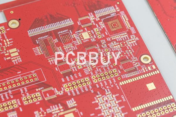
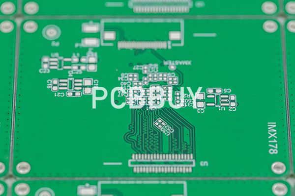
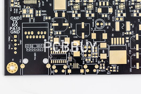
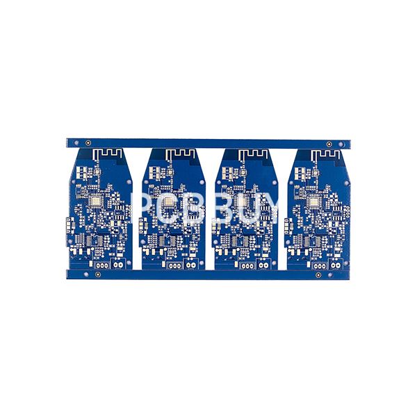
There is much more to choose from since the original green finish. PCB solder masks are now available in a range of different colors and glossy or matte finishes. Selecting different colors will help you distinguish between your printed circuit boards. You can also match your colors to your tastes and palette.
If you are looking for a wider selection of color choices, you may want to go with a glossy finish because it gives you more options.
Green
Black
Red
Yellow
White
Purple
Blue
If you prefer a matte finish, you have fewer options. Currently, only green and black colors are available with the matte finish.
While there is no predominant reason why green is the most common color for solder masks, its popularity could be because it creates the smallest solder dam (space) of all the colors you can choose from. Green is also shown to be most visible to the human eye in daylight, making green PCBs easier to work on, use, and find.
What the solder mask should be used?
An appropriate solder mask depends upon the physical dimensions of the board, components, holes, and conductors, the surface layout, as well as the final application for your product.
You will need a photoimageable solder resist for most modern PCB designs. The surface topography will depend on whether to use a liquid or dry application. And a dry application is that lay down a uniform thickness across the entire surface. But it will be the best for dry mask adheres of your PCB surface is very flat. And if there are complex surface features, you’d better select with a liquid (LPISM) so that there will be a better contact with the copper of your traces and the laminate.
What is the importance of solder mask of PCB?
1. It prevents oxidation of the copper traces.
2. Special PCB inter-connectors are used at particular places on the PCB to connect one layer of a PCB to another. Any other kind of connection is unwanted. Since, the layers are very close to one another; even the smallest bump of solder could cause unneeded connections between the layers. At this point, a layer of polymer, which is the solder mask, helps greatly in making sure that the solder doesn’t provide unnecessary connections.
3. It prevents unexpected connections between components even where tolerances are tight.
4. Solder mask keeps dust and dirt away from the electric connections and the substrate.
5. It prevents the electric connections from corroding.
Solder mask is used for both hand as well as automatic assembly. It is an essential step in the entire process of PCB fabrication. For efficient connections and performance, solder mask is of immense importance.
Industry Category


