How to choose PCB copper thickness?
By:PCBBUY 05/14/2021 18:07

PCBs are versatile components used across numerous industries and electrical devices. And PCB copper thickness can be a crucial factor in designing the perfect board for your needs?
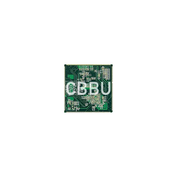
Most printed circuit boards are constructed with 1 oz copper thickness. In PCB manufacturing, if customers do not offer specific specs, we will assume 1 oz when quoting and building the design. If customers have decided that the design requires more current than 1 oz can carry, it would better to consider increasing the copper thickness or increasing the width of your traces. Of course the thicker the copper the higher the cost, but there are certainly times if it is necessary. The cost increase is not only due to the raw material costs but processing thicker copper weights takes more time and is a little trickier to do.
Copper plays an integral role in PCB conductivity, and that is why you need to choose optimal thickness for your application. Take a look at our guide and get to know different weights available, but that is not where we will stop. We will also teach you how to place an order from a reliable manufacturer. So don’t hesitate and start reading now!
How is PCB Copper Thickness manufactured?
The manufacturing of the copper traces of your board, whether on the surface or for internal layers, is done by etching, one of the major PCB manufacturing steps. Layer fabrication begins with a laminate sheet that is completely covered by copper. Etching is the process of removing excess copper from traces and other areas, such as component pads and annular rings for vias, using an ammonia-based solution.
Typically, these sheets begin with preset copper thicknesses. This thickness can be etched down, decreased, or plated up, increased, to the desired specification. Due to the manufacturing process for the sheets, the surface has a degree of roughness that helps with bonding to the dielectric material. However, this can have an increasingly adverse effect on signal integrity at higher frequencies. At frequencies above 100MHz, the skin effect, where current flow is typically near the internal surface of the trace as opposed to through the conductor center, occurs, causing the effective resistance of the trace to increase and oppose current flow.
Traces for plated vias must be added after the holes are drilled. A process for accomplishing this is electrodeposition where the board is placed in an electrolytic solution containing copper ions. A direct current is applied to set up a potential across the via and ions are distributed throughout the via. The distribution of the copper ions throughout the via or the filling determine the quality of signal flow along via traces.
How to choose PCB copper thickness?
Choosing the right copper thickness plays an integral role in circuit board assembly. When considering the thickness of your PCB copper, there are two things to keep in mind. The first element to consider is the barrel’s current capacity for heat rise. The second is mechanical strength, which is determined by the thickness of the copper, as well as the size of your plated-through hole (PTH) and the presence or absence of support vias.
Choosing Materials
There are a number of materials that circuit board assembly services can choose from when designing a PCB. Such options include the standard FR4, which operates at a temperature of 130 degrees celsius. High-temperature polyimide is another option — this material can stand up to 250 degrees celsius.
Tests have been made specifically for circuit board assembly services to find the thermal fortitude of a printed circuit board assembly. Thermal strains come from different PCB assemblies and repair processes. During these times, the distinctions between the coefficient of thermal expansion (CTE) and the PCB laminate drive enough power for crack nucleation as well as the growth-to-failure of the circuit. PCB manufacturers use thermal cycle testing (TCT) to check for increases in a circuit’s resistance while it goes through thermal cycling from approximately 25-260 degrees celsius. Increases in resistance are indications of a reduction in electrical integrity. This is often due to cracks in the copper circuit.
Thermal cycle testing results show manufacturers that the rate of failure can become inadmissible, no matter the material of the board. Studies done on standard boards (FR4 with 0.8-1.2mil copper plating) show that after 8 cycles, 32% of circuit boards fail. Boards with more exotic materials can show impressive improvements to this rate of failure—boards with cyanate ester only have a 3% fail rate.
However, these high-end materials are much more expensive and can cost anywhere from 5 to 10 times more than typical materials. Exotic board materials are also much more difficult to process. These factors make them prohibitive, forcing many manufacturers to use more traditional materials.
Making Your Printed Circuit Board Assembly Efficient
Heavy copper circuit boards can actually eliminate most failures completely. In fact, using a 2 ounce-per-square-foot of copper to plate to a hole wall can reduce the rate of failure to almost zero—this means that a thicker copper circuit is essentially impervious to any stresses that thermal cycling subjects it to.
Selecting the right thickness of copper is essential for a successful PCB assembly project. Making the wrong choice can be detrimental to your design, so it’s best that you work with an experienced manufacturer that can provide expert advice on the best methods of assembly.
Industry Category


