How to design high current PCB?
By:PCBBUY 06/19/2021 17:30

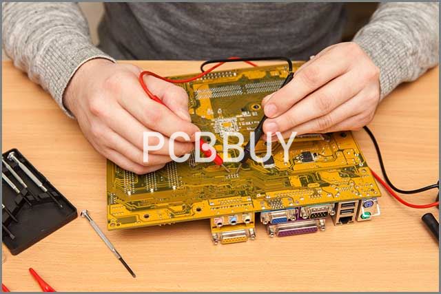
During the PCB manufacturing process, when you need PCB to carry higher currents than usual, what should you do? Moving large currents on PCB requires some design modifications and rules. In this passage, we will provide every detail about designing high current PCB. If you are curious about the topic please read the content below.
What are the basic factors of high current PCB?
As a general rule of thumb, the following are essential fundamental factors for designing a high current board.
Trace Width
One of the primary factors determining how much current a trace can carry will be its width. Traces with higher width will carry more current. Generally, it is a rule of thumb to assume a trace width of 1mm per Amp of current took for a board with standard copper thickness. As you can notice, it soon becomes unreasonable wide when a trace has to carry 10s of amps, and such a path would take up a lot of space.
Copper Thickness
Copper thickness is the actual thickness of the traces that are on a PCB. The default copper thickness is usually 17.5 microns. Higher copper thicknesses can be 35 and 50microns. The higher the copper thickness, the less wide your trace has to be to carry the same current. More increased copper thickness does come at an additional cost but can help save space on your boards since, with higher viscosity, the trace width required is much less.
Manufacturer's Technological Capabilities
As always, you can only design a board that your board manufacturer will be able to manufacture. In high current boards, the following two things are essential and should be looked at on your manufacturer's technical capabilities page.
1. The copper thickness for outer layers - This would mean the two outermost layers on your board, top and bottom. The manufacturer will provide information on how thick(usually measured in microns or oz) they can make the copper on the outer layers.
2. Copper thickness of inner layers - This indicates the copper thickness limits on the inner layers, and often inner layers have to carry large currents, especially for packages such as BGA.
Besides these two factors, one must also look at what kind of temperature grade of board material the manufacturer can offer. Common ones are TG150, TG138, etc.

Heat Produced
Finally, the one factor that will contribute to the longevity of the board and components is the heat that is produced by a high current track on a PCB. The power loss in watts can be calculated as the resistance of the trace multiplied by the square of the current flowing through it. In other words, P= I2R.
This figure ideally should be as low as possible, but even thick traces have a specific resistance, and when carrying large currents, the power loss increases significantly, and the trail heats up. Hot spots in the PCB can then lead to board warping, and layers peeling off and crack developing.
What are the guidelines of high current PCB?
Specific guidelines must follow when arranging high current plates. These are stated and explained below.
Keeping High Current Tracks Short
A long trace will have a more considerable value of resistance. When combined by the fact that it is carrying a large current leads to a significant amount of power loss. Then, power loss can cause a lot of heat, and board life reduces. So it's essential to keep the extensive current paths as short as possible.
Calculating Trace Widths with appropriate Temperature Rise
A width of a trace is a function of parameters such as the current through it, resistance, and the allowed temperature rise. A strict value of the permitted temperature rise is about 10' C. However, this leads to a high trace width. If your design and the board material can handle higher temperatures, then it is possible to have a 20' C temperature rise, leading to a lesser value of required trace width for the same current.
Higher values of allowed temperature rise can use when the product is supposed to use in an environment where the ambient temperatures are not too high.
It is thermally isolating sensitive components from heat.
Many electronics components, such as analog to digital converters, voltage references, and opamps, are sensitive to temperature changes. Their signal can change if the element heats up or cools down. Since high current boards will inevitably produce heat, these components must be thermally isolated to some extent so that they are not affected by the heat produced by the board.
One method to do this is not to have a polygon pour under that component and provide thermal relief connections. Another method is to have board cutouts that separate the sensitive components from parts that produce heat.
What are the design tips of high current PCB?
Here are some design tips for high current boards.
Removing solder mask
It is an inexpensive or rather free method to increase the current capability of a trace, and a path can have its solder mask removed, which then exposes the copper underneath. Then additional solder can be added onto the trail, which will increase its thickness and bulk and lower resistance.
It will then allow more current to be carried by that trace without increasing the trace width or paying extra for additional copper thickness.

Using polygon pours under high current components.
Individual components, such as large FPGAs and Processors, have extensive current requirements and many power pins. They also often come in BGA and LGA packages.
A trick to get enough current to them quickly is to have square polygon pours right under the chip and then having Vias drop down and connecting to them. You can then click the polygon pour to a thick power traces.
Using internal layers for high current paths
If you run out of space for thick traces on the outer layers, it's often an excellent approach to have a solid fill in an internal layer and then using vias to connect to high current devices on outer layers.
Adding copper bars for very high current
In specific applications such as high power inverters and electric automobiles, the current can often be 100A or more. In such cases, it becomes pointless to use traces.
A common practice here is to use solderable copper bus bars that solder onto a PCB's pads and then carry most of the high current. Since the bars are much thicker than traces on a PCB, they can easily take an order of magnitude larger draft than regular hints while having around the same width.
Industry Category


