How to determine PCB trace width?
By:PCBBUY 05/13/2021 17:38
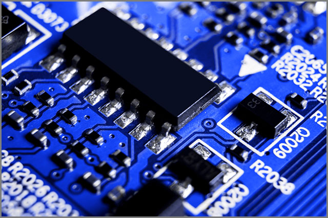
There are several rules and guidelines that will help inform the value of the trace width hen determining trace widths to route a PCB,. With the exception of special cases such as very high frequency signaling and high power applications these rules can be applied to every PCB.
Determining the trace width of your PCB comes down to the fabrication of your board and what it allows. However, there are a few guidelines to follow that will help you get a clearer calculation. The general rule is the greater the trace width, the greater the carrying capacity that prevents overheating.
Why is PCB trace width important?
The relationship between trace width and current carrying capacity in your printed circuit boards is fairly straightforward. Specifically, a cross-sectional area of trace and temperature rise determines your current carrying capacity, with your cross-section of trace directly proportional to copper thickness and trace width.
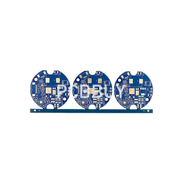
However, this does not necessarily mean that trace carrying capacity is directly proportional to cross-sectional area. Calculating the maximum current that a trace is able to hold based solely on trace width and temperature rise is not always a simple calculation, as you may already have found.
The thicker traces have been optimized for current carrying capacity and are used for peripherals or power-related functions that demand higher power, such as fans, motors, and general power delivery to lower level components.
How to determine PCB trace width?
These trace width calculators will prompt you to enter design specifications such as the thickness of copper, the maximum amperage that will pass through the trace, the length of the trace, and the acceptable increase in temperature due to the resistance of the trace dissipating power. After entering these values you will be presented with a calculated trace width. It is important to note that this value is a minimum width required to meet the design criteria inputs.
Now, a PCB trace acts as a resistor and the longer and narrower the trace, the more resistance is added. If we assume some general things like a 1-ounce copper pour and ambient room-temperature during normal operation, we have what we need to calculate both the minimum trace width and expected voltage drop at that width.
What is Trace Spacing?
The size of a PCB is directly connected to the cost of the PCB, so in general PCBs are kept as small as possible. The downside of reducing board size is that it can limit the available space to route traces. For low power signal traces it is generally advised to keep traces small to increase the available space available for routing. Excessively large traces consume valuable PCB space while offering highly diminished returns. 6 to 30 mils is typical for most signal trace widths.
What is Trace Termination?
The point at which a trace meets a pad can also inform the width of a trace. In most cases, trace widths are set to the same width as the pad they terminate to. This will help aid with routing traces away from the component they connect to and will avoid violating spacing between adjacent traces.
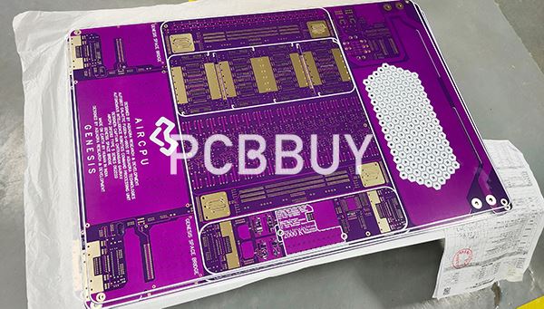
Determining the width of a trace based on the current demands is important for most power traces and high power signals, however, most traces on PCBs pass signals which draw negligible current. For these low power signal traces, we must look at other characteristics of the PCB to determine the width.
The main factor being current handling. But what determines the current handling of a track is actually how much you want to allow it to rise in temperature. This is commonly called a Joule Heating problem.

Basically the research went like this. Copper foil used on PCBs comes in fairly standard thicknesses - typically measure in ounces per square foot (gee thanks, legacy imperial system!) But so you know, 1oz copper is about 1.4mils (thousandths of an inch) or 35μm thick. So the scientists would make single-sided PCBs with tracks of length around 1 inch, and various known widths. Using clever instruments, they measured the change in temperature in the middle of each trace with a range of fixed currents, and plotted the results on an X-Y chart. Then they applied a power-law or logarithmic curve-fit to find some functions that accurately predict the temperature rise for a given cross-sectional area of relatively long traces for a given fixed current.
Industry Category


