How to do PCB testing?
By:PCBBUY 05/19/2021 18:10

PCB testing is essential in ensuring quality products during the design and manufacturing processes. It avoids situations where designers and manufacturers realize that the product is faulty at the last minute, while the boards are in full production, or already in the market.
Even after following proper design and manufacturing processes, there is always a risk of defects, bugs, human errors at the prototype stages. Identifying and addressing these issues before the final product is critical in ensuring the performance, functionality, and reliability of the products.
Why PCB testing is important?
Testing is a crucial part of the development cycle for PCBs. When PCB testing is conducted throughout the production cycle, it can help save money and prevent issues when it comes to the final production run.
Some design analysis techniques can be used during the early stages to help minimize major issues during the manufacturing process, but there’s also a wide range of PCB product testing methods that can be used on physical boards. These tests, run on prototypes or small-scale assemblies, look most closely at potential shorts, solder joint issues and functionality, ensuring that each tested PCB will function as intended.
What are benefits of PCB testing?
Bug identification: The primary benefit of PCB testing is that it helps identify problems in PCBs. Whether the issue lies in functionality, manufacturability or elsewhere, PCB tests identify issues in a PCB design so that designers can adjust accordingly.
Time savings: PCB testing in the early stages can help save time in the long run, allowing designers to identify major issues during the prototyping stage. Thorough testing enables designers to determine the root cause of each problem posed quickly and easily, making adjustments so that they can move on with production at a faster rate and reduce product lead-time.
Cost reduction: PCB testing prevents wasteful production of faulty products by using prototypes and small-scale assemblies to test the products. By completing thorough testing early in the design process, designers can prevent wasteful full-scale assemblies of faulty PCBs, ensuring that the design is as flawless as possible before it goes into production. This step helps to significantly reduce production costs.
Fewer returned products: When companies conduct PCB testing, they lower the chances of selling defective products or those that don’t meet performance standards. As a result, they don’t see as many returned products, leading to reduced costs associated with refunding customers and handling defective goods. Additionally, having fewer returned products can result in higher customer satisfaction and an improved company reputation.
Increased safety: Since PCBs are often used in essential electronic technologies, their failure can cause major issues for a company’s productivity or an organization’s ability to perform essential services. A defective PCB could cause a fire, potentially putting those near it in danger. Testing prior to manufacturing can also ensure machines and workers aren’t damaged or injured due to an improper design during production.
While thorough testing isn’t necessary for all types of PCBs, especially matured products well into their product life cycle, the majority of new PCB designs need robust and frequent testing of the design process. By establishing an appropriate PCB testing procedure for your organization’s needs, you can experience the benefits of PCB testing.
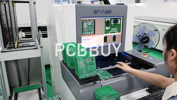
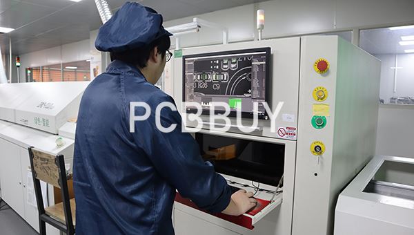
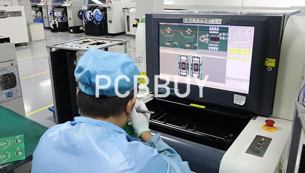
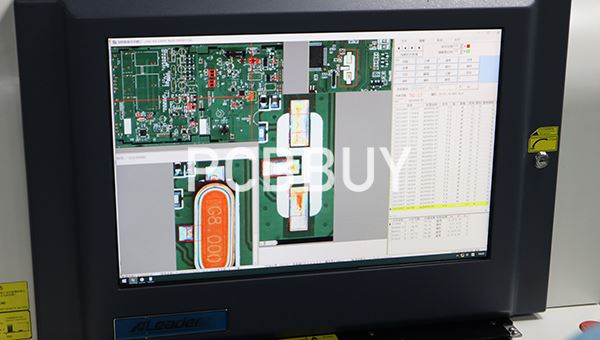
How to do PCB testing?
Start with a Visual Inspection
When a circuit board suddenly stops working, there are sometimes obvious signs of what went wrong. You’ll need to rely on your vision to spot faulty components or broken traces. Often, circuit boards deployed in the field are damaged by electrical surges and there are telltale signs on the PCB.
Look for a burnt spot, particularly on the power supply module or I/O and connectivity ports. Pay attention to cracked ICs, broken traces, and blown capacitors. Sometimes, you could trace the damaged components by their acrid scent.
Check the Power Module
Measure the voltage of the power rails with the multimeter. Both the input and output of the voltage regulator need to show the expected values.
Check the fuse if the input voltage measured at the voltage regulator is 0V. If the fuse is replaced and immediately breaks after power-up, it means other components are shorted and draining a huge amount of current.
A voltage of 0V, or below Vcc, at the output often means that the regulator or a component along the voltage rail has a short circuit. If that’s the case, the damaged component will heat up quickly. Bring your hand close to the components to feel if one is giving off excessive heat. Be careful to not directly touch the component when it’s powered on, as it can be extremely hot.
Remove the overheated components and confirm that the voltage has returned to the expected value. If voltage observed is still different than the expected voltage, there could be more components that are damaged down the voltage line. Refer to the schematic and remove the next component that is near the edge of the PCB.
If there aren’t signs of overheated components then look for broken traces. A broken trace could result in the voltage being detected at some points of the trace but not in others. Use your multimeter to narrow down where the discontinuity is.
Check the Input/Output Ports
If the I/O is protected by fuses, Zener diodes, or varistors, ensure that they are functioning well. The logic IC or the microcontroller is likely damaged. The only way to find out is to replace the parts with good ones.
Check Communication Ports
Circuit boards with communication ports like Ethernet and RS485 have an increased risk of failure. When communication failure is detected, check for burns or cracked communication ICs or protective components like Zeners.
Industry Category


