How to layout PCB?
By:PCBBUY 05/13/2021 17:43

The layout process of your PCB is a very important part to creating a reliable, cost-effective board. It is always necessary to make sure you leave enough time for PCB layout, though PCB design and component selection are also essential. There are several factors of determining the optimal PCB layout design, especially since today’s boards are becoming more complex, compact and lightweight. The growing popularity of flexible PCBs complicates the process, too.

Consider the importance of PCB layout affairs or you will fail to finish a design that doesn’t translate well to the real world. Besides, if you don’t manage the layout correct the first time around, you will need to restart the process, which can cause manufacturing delays and added costs.
In this passage, we are talking about how to layout PCB and the tips during the process. We will look at the steps of PCB layout and considerations. Let’s start it.
What is the PCB layout process?
Since PCB layout is very important of the PCB manufacturing process, we will see the layout steps to know how it is designed before produced. The process includes the steps below:
What is Concept?
After identifying the need for a PCB, the next step is determining the board’s final concept. This initial phase involves defining the functions the PCB will have and perform, its features, its interconnection with other circuits, its placement in the final product and its approximate dimensions. Also, consider the approximate temperature range the board will operate in and any other environmental concerns.
What is Schematic?
The next phase is to draw the circuit schematic based on the final concept. This diagram includes all the information needed for the electrical components of the board to function appropriately, as well as details such as component names, value, rating and manufacturer part numbers.
While you’re creating your schematic, you’ll be creating your bill of materials. This BOM contains information on all of the components you need for your PCB. Always keep these two documents up to date.

What is Board-Level Block Diagram?
Next, you will complete a board-level block diagram, a drawing describing the final dimensions of the PCB. Mark areas designated for each block, sections of components that are connected for electrical reasons or because of constraints. Keeping related components together will enable you to keep your traces short.
What is Component Placement?
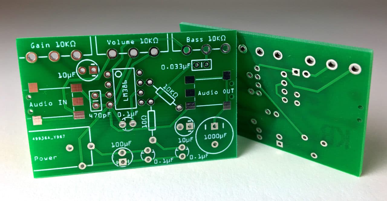
The next step is component placement, which determines where you will place each element on the board. Often, you may go through several rounds of refining component placement. circuit board component placement
What is Testing?
After you’ve completed the design, you should conduct a series of tests to ensure it meets all your needs. If it does, the design is complete.
What are the PCB layout guidelines?
There are lots of considerations during the PCB layout and design process, so we are going to provide the guidelines for you to reference.
Board Constraints
Some of these basic constraints include the size and the shape of the board. The standard PCB is rectangular. You will need to ensure you have adequate board area for the circuit. The size of the end product, the functionality the board must provide and other factors determine how large the board should be. Before you start the design process, estimate the size of the board. If you do not have enough space for all the functionality required with a more straightforward design, you may need to use a multilayer or high-density interconnect design.
PCB Constraints
Another critical consideration is the number of layers you’ll need, which power levels and design complexity will help decide. Adding more layers may increase production costs but enable you to include more tracks. This may be necessary for more complex boards with advanced functionality.

Use at least two vias to make layer transitions for all high-current paths. Using multiple vias at layer transitions increases reliability, improves thermal conductivity and reduces inductive and resistive losses.
Manufacturing Processes
You’ll need to use reference holes or points that work with the manufacturing process on the board. Always ensure holes are clear of components. Also, keep the board mounting method in mind. Different approaches may require you to leave different areas of the board open. Always check with your fabricator to make sure they have the capabilities to produce the type of board you need.
Materials and Components
You’ll first need to make sure the desired items are accessible. Some materials and parts are hard to find, while others are so expensive they’re cost-prohibitive. Different components and materials may also come with different designs needs.
Component Placement Order
One of the most fundamental PCB design guidelines involves the order in which you place components on the board. The recommended order is connectors, then power circuits, then precision circuits, then critical circuits and then the rest of the elements.
Orientation
When you are placing components, try to orient those that are similar to one another in the same direction. This will make the soldering process more efficient and help prevent mistakes from occurring during it.
Placement
Try not to place parts on the solder side of the PCB that will sit behind plated through-hole parts.
Industry Category


