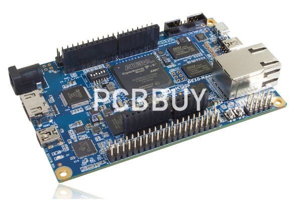
How to make FPGA PCB?
By:PCBBUY 06/04/2021 17:28

A field-programmable gate or grid array is a little more complicated than a microcontroller. Most of the time, a chip comes pre-programmed. As the user, you can change software, but not hardware. This brings us to the defining element of an FPGA — you, the user, can configure its hardware after purchase.
Engineers find this especially useful for prototyping their own application-specific integrated circuits. In fact, Intel uses a form of FPGA to streamline their own prototyping process. FPGAs are also useful because the devices in which FPGAs are embedded can be altered without needing all-new hardware.
Engineers find this especially useful for prototyping their own application-specific integrated circuits. And in this passage we will talk about all the details of FPGA PCB.
How does FPGA PCB work?
FPGAs have an “array” of integrated hardware circuits — these arrays are groups of programmable logic blocks. During manufacturing, an FPGA has not been configured to have any particular function. Instead, the user can configure it and later reconfigure it however they choose.
The user does this using a hardware description language (HDL). An FPGA has logic blocks, like AND and XOR, which the user can piece together with interconnects. Modern FPGAs have many logic gates and RAM blocks, so they can accommodate complex computations. Some FPGAs also have analog-to-digital converters or digital-to-analog converters, similar to field-programmable analog arrays (FPAAs).
What are the features of FPGA?
They require more skill to use: You’ll need more than a basic understanding of coding language to program an FPGA. In addition to knowledge of a coding language, you’ll need to be able to track mass amounts of variables. You’ll also need to understand a hardware description language. Designing and redesigning hardware is not a task for beginners.
They allow for more parallelism: An FPGA has thousands of logic blocks, all of which you can program. You can create processes independent of one another, decreasing instances of bottlenecking as with microcontrollers.
They allow for a higher level of customization: Simply put, if you know what you’re doing, you can do a lot more with an FPGA than a microcontroller. If you want to program something complicated, you’ll need more customizability than a microcontroller provides.
They tend to cost more: One drawback of FPGAs is that they tend to be more expensive than microcontrollers. Despite higher upfront costs, they can save money for industries that may need to make retroactive changes — think of the rear-view camera example.
They’re ideal for more complex applications: Because FPGAs allow for parallel processes, you can implement more inputs with an FPGA than with a microcontroller, without running into a bottlenecking issue. This makes them ideal for more complex operations.
They allow for later alteration: One of the biggest benefits of an FPGA is that the hardware itself can be changed after its initial programming. For this reason, you can change a device’s function without completely replacing its hardware. This is more cost-effective in the long run, especially for mass-producing industries.
How to make FPGA PCB?
The normal steps I follow are: Find a COTs board and get a rough idea of the internal FPGA resources you will need, in particular I pay attention to:
LUT (look up table) count
Use this rule of thumb. If the design is nearly finished take the size of the design (LUT count) and find an FPGA with at least 30% more LUTs. if the design is not close to finished go up to 50% or 100% more LUTs. So if the design fits into 9K LUTs make sure to use an FPGA with 12K LUTs or greater. I tend to go overkill and probably would go up to 25K LUTs. This will save you excruciating headaches later. Whomever is commissioning this board design should understand that there should be more than one spin of this design so it is understandable to oversize the first version of the FPGA. There are a lot of available FPGAs that have different LUT counts in the same package size so for example the Xilinx Spartan 6 LX45 Package is the same as the LX75 so you can start out by using a the LX75 (75K LUTs) and if your design easily fits into less than 40K LUTs then you can save costs on the design with just a BOM Change.
BRAM (Block RAM count)
Determine if your design requires more memory resources than your FPGA has internally. This is easily overlooked at first but in a design you tend to use block RAM for various reasons (ROMs, FIFOs, etc...) I ran out of block memory on a design and attempted to use distributed RAM (using the LUTs as RAM) and it ate up all my LUTs very fast. It's important to determine if you will require external memory. This adds a lot of risk to designs because if the design requires any level of performance you can't just use an external SRAM or SDRAM as your memory because their data transfer rates from these components are terribly slow compared to the speed at which you can move data around in your FPGA so the only comparable way to move data is with DDR2 and DDR3 and if you have to use these you add risk due to mistakes in schematics and layout and more work for the HDL team.
Enumerate all signaling standards and possible voltage levels your will use: This is important because some of the signaling standards you wish to use (LVDS, LVSPEC, LVCMOS) may have voltage restrictions. Go through the user guides and make sure all these standards are supported.
Power supply requirements
I sympathize with all the previous gripes about undersized power supplies getting the core voltage spec'ed is tuff, lately I have been using a lot of TI Nano modules for the large but low end FPGAs (Spartan LX45(T) - LX75(T) and Lattice ECP3). Fortunately you can mitigate some of the risks on when sizing the power supplies used for the I/O. In particular if this bank is not driving an unknown source (expansion connector) then the process is as follows: Find all the components that this bank will attach to, determine the input capacitance for all of those components, find out the maximum clock rate you will be driving these signals then you can calculate both the power requirement and roughly estimate the bypass requirement, although a lot of the FPGA manufacturers have been putting on the minimum bypass capacitor requirements in something like the DC Switching Guidelines.
Industry Category


