How to make PCB via?
By:PCBBUY 05/12/2021 17:50
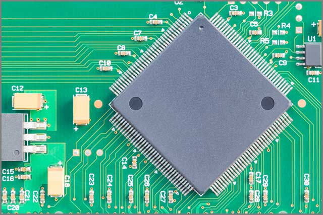
In order to pass an electrical signal from one layer to another, designers used something called a via. For the PCB designer, a “hole” in the board is for thru-hole component pins to be inserted into and soldered. There may also be larger holes for attaching mechanical objects with bolts or other fasteners that may or may not be soldered. But for all of those other small holes that didn’t host a pin, they were called via.
What is a PCB via?
A via is a plated-through hole in a PCB that you can use to route a trace from your board's surface layer to the inner and other layers. It is essential to realize that you can drill PCB vias mechanically, and you can plate them to create electrical connections.
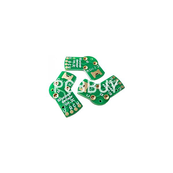
Vias are vital in multi-layered boards, which are challenging to design and produce. They create routes for the sufficient flow of electrical and thermal current between the board's different layers. In brief, vias are basically "channels" that vary in size and type.
Why we use via in PCB?
If you have a simple circuit board, you may not need vias. But you need vias when you are dealing with a multi-layered board, as mentioned earlier.
Vias will help to establish an excellent component density in multi-layered boards. Besides, they also raise trace density in multi-layered boards as you can run them over and beneath each other in different directions. Vias allow the various traces to link with each other. In this case, they act as vertical connection factors. If it is fail to incorporate vias into a multi-layered PCB routing process, you will end up placing your components densely.
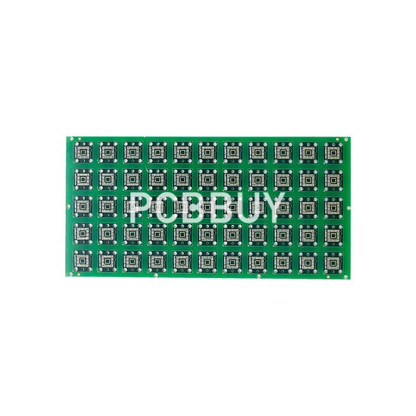
Lastly, you need vias to facilitate the transmission of signals and power between layers. If you do not want to use vias, you should route your PCB components on a single plane. And the surface mounted parts in a multi-layered PCB make it impossible to route components on a single plane.
How to make PCB via?
Vias are plated along with the rest of the circuit board during its regular fabrication process. Micro-vias are different in that they are laser drilled and depending on which layers they are on, the process will vary. There are also different processes for blind and buried vias as well. But for standard thru-hole vias, the process can be summarized like this:
Vias are plated along with the rest of the circuit board during its regular fabrication process. Microvias are different in that they are laser drilled and depending on which layers they are on, the process will vary. There are also different processes for blind and buried vias as well. But for standard thru-hole vias, the process can be summarized like this:
Once the different board layers have been composited together, all of the thru-holes are drilled. This includes component pin holes, non-plated holes, and vias. The holes are cleaned of debris from the drilling operation. This can range from burrs on the edge of the holes, to resin residue inside the holes. A combination of abrasive mechanical and chemical processes is used for this.
A thin layer of copper coating is added chemically into the holes and onto the surface of the board through a process called electroless copper deposition. This gives the copper plating a base to build up from. The full amount of copper is now electroplated on the exposed metal areas of the board, including in the via holes. This is done by connecting the board to an electrical charge so that the boards act as cathodes for the electroplating process, and then dipped in chemical baths.
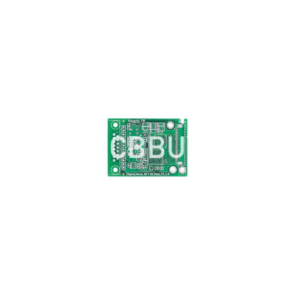
The board goes through numerous baths for cleaning and plating, and the entire process is tightly controlled to make sure that an even amount of copper is produced. The chemical solutions and the process are designed to have a good “throwing power” in order to evenly plate copper within the via holes. Once the copper is fully plated on the surface of the board and in the holes, tin is plated on top of that as an etch resist.
Finally, any area of copper not protected by tin is etched away to leave only the desired traces, area fills, and of course the plating in the via holes.
There are many other aspects to fabricating a circuit board that we have left out of this list. These would include screening images onto the board layers, preparing the inner layers for compositing, and applying solder mask to name a few. But this will give you the basic process for how vias are plated.
Industry Category


